Longreads
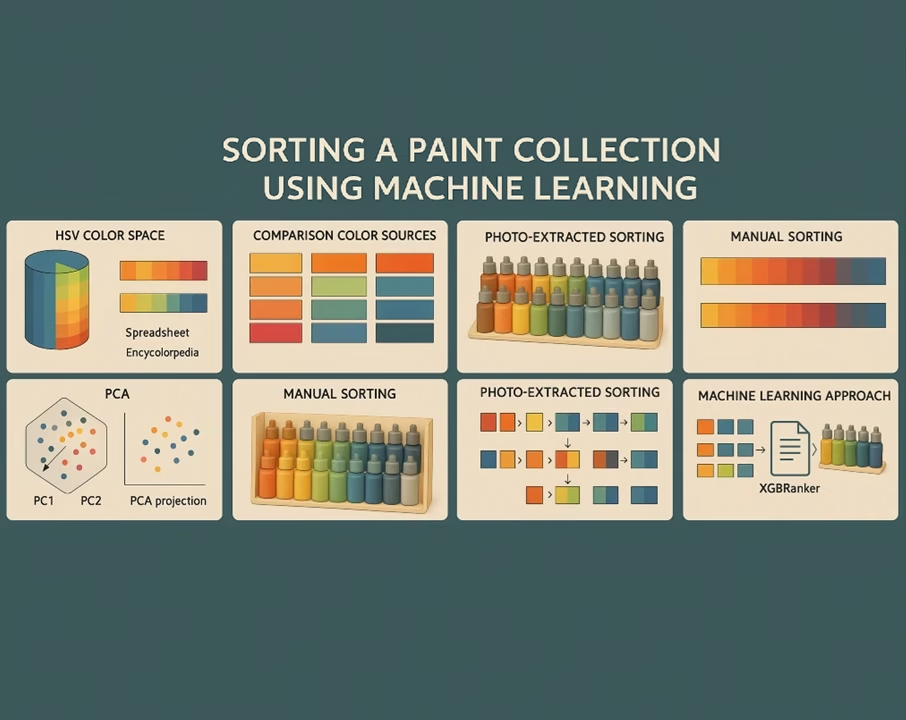
Sorting Vallejo Paints with Machine Learning
This article explores how to visually sort color collections using both statistics and machine learning. After experimenting with PCA for dimensionality reduction ...
K-Means Clustering for Colors
Discover how K-Means clustering helps analyze and evaluate Vallejo Model Color paints using Rembrandt’s masterpiece as a case study. Learn to identify ...
HSV color chart for vallejo paint
Curious how your paints stack up in color space? I analyzed my Vallejo paints by converting RGB values to HSV, visualizing them ...
Editor's Choise
No items were found matching your selection.
PID control on PIC microcontroller
For decades, the PID control system has stood as one of the industry's most established and widely adopted strategies, owing to its straightforward yet efficient algorithm. Within this ...
Subscribe for the daily Newsletter
Our biggest stories, delivered to your inbox every day.


