


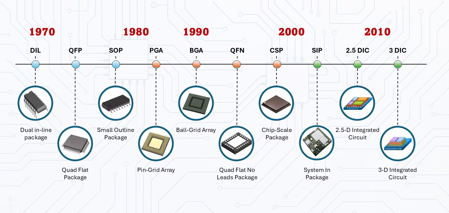
Semiconductor Packaging Technology
Wire bonding and flip-chip packaging represent two fundamental approaches to chip interconnection. While wire bonding offers simplicity and cost benefits, flip-chip allows ...

Scaling beyond 100nm – Nanoelectronics Era
As silicon and silicon dioxide reach their scaling limits, engineers turn to high-k materials, metal gates, and new device architectures like FinFETs ...

Scaling of CMOS: Microelectronics era
As CMOS technology shrank below 1 μm in the microelectronics era, high electric fields caused reliability issues like hot carrier effects. Techniques such ...

Beyond Conductivity: Advanced Metal Science
Explore the advanced physics of metals beyond conductivity. Learn about superconductivity, AC conductivity, and electromagnetic interactions.


