

In this tutorial, we will discuss how to interface a 74HC595 Shift Register with a PIC microcontroller. The 74HC595 is a popular integrated circuit (IC) that serves as a shift register with output latches. It is often used in digital electronics and microcontroller projects to expand the number of output pins available.The “74HC” prefix indicates that it’s a part of the 74 series of logic chips and “595” is its specific model number.
What is a 747HC595 Shift Register?
The 74HC595 has an 8-bit shift register, which means it can store and shift out 8 bits of data serially. It can accept data one bit at a time and shift it through the internal register. The data is shifted into the 74HC595 through a single data input (DS or SER), which is connected to a microcontroller or another digital source. The data is then latched and stored in the internal registers. The 74HC595 has an output latch that holds the data in parallel form after it has been shifted in. This means that you can load the shift register with data and then latch that data to the outputs all at once, rather than shifting it out bit by bit. And finally, multiple 74HC595 chips can be cascaded together, allowing you to control even more output pins using a single microcontroller output.
The 74HC595 is primarily a digital logic IC designed for signal processing and data manipulation, so it’s not intended to handle large currents directly. Each output pin (Q0 to Q7) of the 74HC595 can typically source or sink around _6 mA – 8 mA_ of current. This current rating is meant for driving low-power components like standard LEDs or small-signal transistors. It requires a power supply of _5V_, hence you can use the same power supply that you use for the microcontroller.
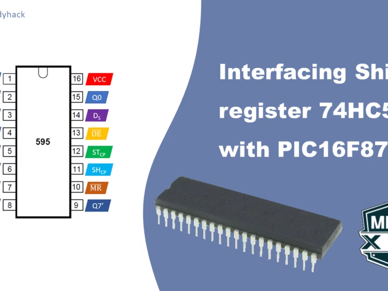
Pin diagram
The Shift Register is a 8-bit shift register with 16 terminals, as shown here below. Terminals Q0 to Q7 are the outputs, Q7′ can be used to daisy chain more shift registers, and the rest of the pins are to configure this component.


Understanding Shift Registers
Here’s a basic explanation of how a shift register works:
- _Serial Input (DS)_: When you want to input data into the shift register, you send a series of binary values (0s and 1s) one bit at a time to the Serial Data Input (DS) pin. Each time you provide a clock signal (SHCP), the next bit is shifted into the shift register. The data shifts from one flip-flop to the next, effectively moving through the register.
- _Shift Clock (SH_CP)_:The Shift Clock input controls the timing of the shifting process. On each rising or falling edge of the clock signal, the data moves from one flip-flop to the next in the shift register. This action allows the data to propagate through the entire register.
- Output Latches and Parallel Output: The shift register typically has an internal set of latches. These latches allow you to capture the shifted-in data and hold it temporarily. The _Latch Clock (ST_CP)_ is used to transfer the data from the internal storage (shift register) to the output latches. This is often done to ensure that all output pins change simultaneously, reducing any flickering or visual artifacts in applications like driving displays.
- _Parallel Output (Q0 to Q7)_: Once the data is latched into the output latches, you can read the binary values from the parallel output pins _(Q0 to Q7)_. Each pin corresponds to one bit of the data that was shifted in.
- Cascadeability: In some shift registers, like the 74HC595, there’s an additional serial output pin _(Q7′)_ that allows you to cascade multiple shift registers together. This lets you chain multiple shift registers so that the output of one shift register feeds into the input of another, effectively creating a longer shift register with more storage capacity.
Creating a circuit with 74HC595
In this illustrative example, we interfaced the PIC16F877A microcontroller and the 74HC595 Shift Register. It’s important to note the intentional decision to maintain diverse naming conventions for the components. This strategic approach takes into account the potential variability in designations that might arise from different manufacturers. It’s worth highlighting that despite these naming differences, the core pin configuration remains consistent. If nothing helps, follow the connections between the numbers of the pins in the schematic.
To elaborate further, the correspondence can be summarized as follows:
- _Q1 – Q7 ⟶ QA – QH_
- Latch clock _ST_CP ⟶ RCK_
- Serial Data _DS ⟶ SER_
- Clock pulse _SH_CP ⟶ SCK_
- _¬OE ⟶ G_
- _¬MR ⟶ SCL_
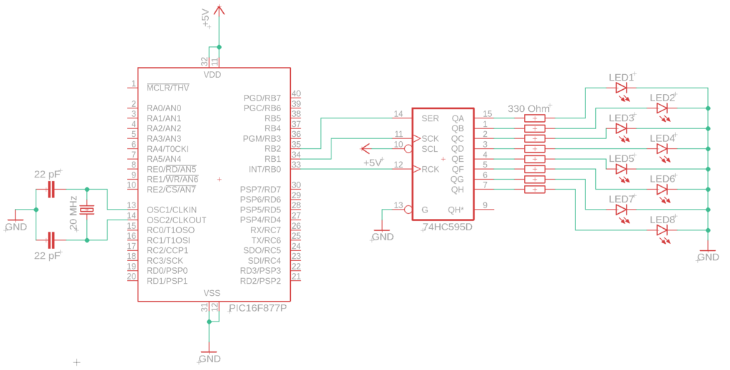
This code is to interface the PIC16F877A with the 74HC595 Shift register, so it can control 8 LEDs with only 3 connections.
					#define _XTAL_FREQ 20000000 // Define crystal frequency to 20 MHz
#include <xc.h>

// Configuration bits settings
#pragma config FOSC = HS        // External Oscillator (HS)
#pragma config WDTE = OFF       // Watchdog Timer Disabled
#pragma config PWRTE = ON       // Power-Up Timer Enabled
#pragma config BOREN = OFF      // Brown-out Reset Disabled
#pragma config LVP = OFF        // Low-Voltage Programming Disabled

void shiftOut(unsigned char data) {
    for (int i = 0; i < 8; i++) {
        RB2 = (data >> i) & 0x01; // Set LSB data on bit RB2, ready to be sent on next clockpulse
        RB1 = 1; // Clock pulse
        __delay_us(500);
        RB1 = 0;
        __delay_us(500);
    }
    RB0 = 1; // Latch data
    __delay_us(500);
    RB0 = 0;
}

void main(void) {
    TRISB2 = 0; // Set RB2 as output (DS / SER)
    TRISB1 = 0; // Set RB1 as output (SH_CP / SCK)
    TRISB0 = 0; // Set RB0 as output (ST_CP / RCK)

    while (1) {
        // Shift out data to control LEDs
        shiftOut(0b01010101); // Turn on the odd LEDs
        __delay_ms(250); // and wait

        shiftOut(0b10101010); // Turn on the even LEDs
        __delay_ms(250); // and wait
    }
}
The “shiftOut” function in the provided code is used to send data to the 74HC595 shift register. It performs a serial data transmission by sequentially shifting each bit of the data byte into the shift register and then latching the data to the output register of the shift register. This allows you to control multiple digital outputs using only a few microcontroller pins.
Here’s a step-by-step explanation of how the shiftOut function works:
Function Definition: The
shiftOutfunction is defined to take anunsigned charparameter nameddata, which represents the byte of data you want to send to the shift register.For Loop: The function contains a
forloop that iterates fromi = 0toi = 7. This loop will iterate through each bit of thedatabyte.Serial Data _(SER)_: Inside the loop, the line
RB2 = (data >> i) & 0x01;shifts thei-th bit of thedatato the least significant position (shifts it every loop one bit further to the right) and then masks it with0x01(binary00000001). This sets the value of the least significant bit ofdatato theSERpin (RB2). This is how the individual bits of the data byte are sent sequentially to the shift register.Shift Register Clock _(SCK)_: After setting the bit of data on the
SERpin, the lineRB1 = 1; RB1 = 0;generates a clock pulse by setting theSCKpin (RB1) high and then low. This clock pulse causes the shift register to shift the data into its internal shift register. The delay (of 500 microseconds) between clock pulses and latches is important to ensure that the data is correctly shifted into the shift register and then properly latched to the output pins.Latching Data _(RCK)_: Once all bits have been shifted, the line
RB0 = 1; RB0 = 0;generates a latch pulse by setting theRCKpin (RB0) high and then low. This pulse causes the data in the shift register’s internal register to be transferred to the output pins, thus updating the states of the connected devices (LEDs in this case).
Summary
In this tutorial we learned what a shift register is, its pin diagram and its function. We learned how to interface it with the microcontroller PIC16F877A so it can drive 8 LEDs using only 3 lines. We have seen the code to program it, and in particular the shiftOut function and its exact working.
Florius
Hi, welcome to my website. I am writing about my previous studies, work & research related topics and other interests. I hope you enjoy reading it and that you learned something new.
More Posts


Comments
This actually answered my downside, thanks!
I’m happy I could help you out!