

I needed a business card, but the idea of handing out a flimsy piece of paper with just my name on it felt boring. As an engineer, I knew I could do better. The solution came quickly: why not turn a printed circuit board (PCB) into my business card? After some research and inspiration from others who tried it, I decided to design my own PCB business card with a feature called NFC. In this article, I’ll walk you through the choices I made and the reasoning behind the design.
Table of Contents
In the first part I explain what NFC is, how it works and what to pay attention to. The next part goes into antenna design and the calculations behind it. The final part focuses on the supporting circuitry and shows how everything comes together in the finished business card.
What is NFC?
NFC stands for Near Field Communication, and is a short range radio technology that enables communication between two devices at close proximity. NFC standards support different data transmission rates up to 424kbit/s, and operates at 13.56 MHz.
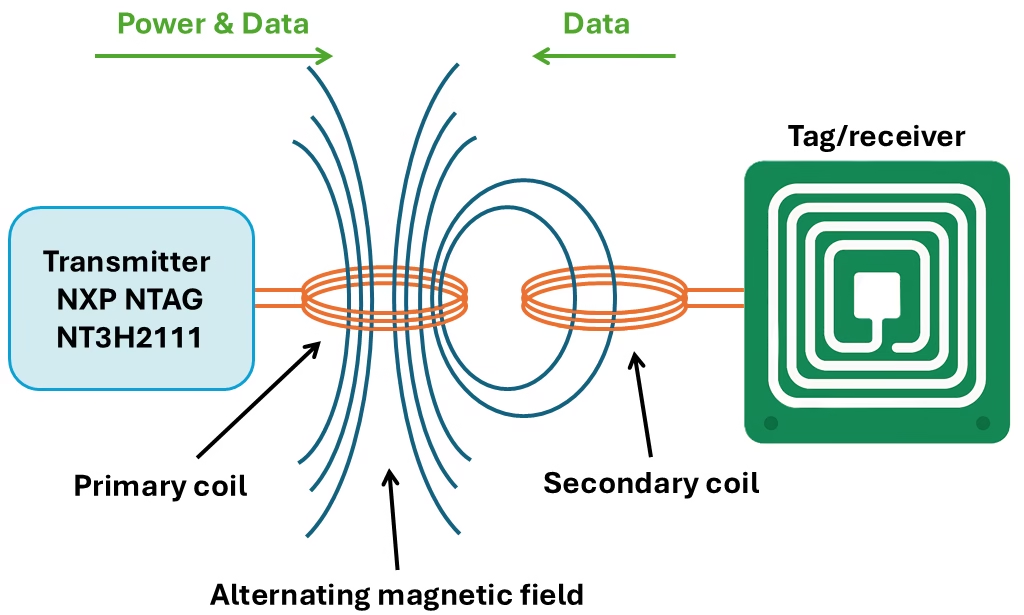
Similarly to RFID, there is a master and slave part. In this case, there is an emitter (or reader/writer) and a tag (i.e. a card). The emitter generates an RF field that powers a passive tag using electromagnetic induction between the two loop antennas. The reader coil acts as the primary winding, generating an alternating magnetic field at 13.56 MHz. The tag coil acts as the secondary winding, where the changing magnetic flux induces a voltage that powers the tag’s chip. Because the coupling is weak, only short distances are possible. Communication is achieved by the tag varying its load, which causes detectable changes in the magnetic field that the reader interprets as data.
NFC Chip
For this project I use the NXP NTAG NT3H2111W0FTT NFC IC. There are several reasons for this choice. The chip is easy to configure and test using NXP’s mobile app. NXP also offers free samples of their chips, which allowed me to evaluate the device without upfront cost. More importantly, the NTAG meets the specifications required for my design. Its key features include energy harvesting up to 15 mW (under ideal conditions) and zero-power operation with non-volatile data storage, which are particularly useful in this application.
From a packaging perspective, a smaller XQFN package would have been preferable, since its thickness is roughly half that of a TSSOP. However, because this project is just to show what I have done and other components (such as the LED) are of similar size, so I picked the TSSOP package. It is easier to solder and to rework if I get into any issues.
Additional important specifications of the NT3H2111W0FTT are:
- Contactless transmission of data at 106 kbit/s
- ISO/IEC 14443A compliant,
- 64 bytes SRAM buffer for transfer between NFC and other peripherals through I2C,
- 2k bytes EEPROM,
- Input capacitance of 50 pF
Calculations & Antenna Design
The NFC tag consists of two main parts: the IC and the antenna. The NTAG IC can be represented by the open terminals LA and LB, with an internal resistor RIC and the input capacitance CIC.
The antenna can be modeled by a inductance Lpc parallel to a loss resistance Rpc of the copper, and the antenna capacitance CC. This capacitance arises from both the inter-turn capacitance and any deliberately added tuning capacitance (discussed later).
The connection between the IC and antenna introduces its own series resistance Rcon and parasitic capacitance Ccon.
Together, the IC capacitance, antenna capacitance, and connection capacitance form a resonant circuit with the antenna inductance. The internal resistance, combined with the antenna loss resistance and connection resistance, determines the quality factor of the tag. For very small connection resistance (Rcon << 1Ω), the equivalent circuit can be simplified.
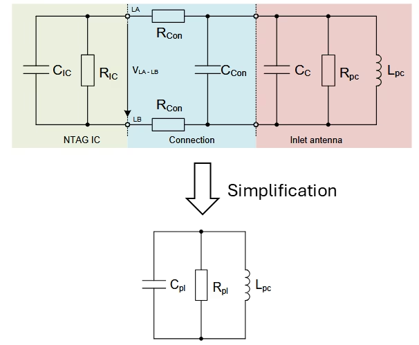
The parallel equivalent capacitance of the tag becomes
\[C_{pl} = C_{IC}+C_{con}+C_C\]
and the parallel equivalent resistance becomes:
\[R_{pl} = \frac{R_{IC}\cdot R_{pc}}{R_{IC}+R_{pl}}\]
Resonance frequency and Quality factor
Based on this simplified model, we can calculate the resonance frequency fR of the IC [1]:
\[f_R = \frac{1}{2\cdot\pi\sqrt{L_{pc}\cdot C_{pl}}}\]
The value depends on the input capacitance, which depends on the input voltage VLA-LB. Therefore, the resonance frequency depends on the input voltage of the IC.
Similarly, with the simplified model, the quality factor Q can be calculated:
\[Q= \frac{R_{pl}}{2\cdot\pi\cdot f_{op}\cdot L_{pc}}\]
Estimation of Electrical Parameters
For operation, tuning slightly above 13.56 MHz would lead to a maximum read/write distance. NXP recommends up to a frequency of 14.5 MHz.
In order to calculate the approximate inductance of the antenna, it is necessary to estimate the total capacitance of the system.
- The antenna capacitance CC depends on the type of technology used, but is normally around 2-4 pF.
- The connection capacitance Ccon ≈ 0.5 – 2 pF.
- And from the specs of the NT3H2111 chip, we can conclude that the nominal capacitance CIC = 50 pF (but there is a +/- range).
You can tune the resonance frequency further by adding an additional capacitor in parallel to Ccon. In a later section where I explain the schematic, I call this the tuning capacitor (C1), and in my PCB design there are two slots for it for testing purposes.
Antenna Design
For the antenna design (the inductor coils), there are several options, which I list out in this section.
Option 1: Calculating the Antenna Inductance
At its core, inductance is just the magnetic field captured by the coil, divided by the current that made it. For a flat spiral coil (antenna), this comes down to three important parameters:
- The number of turns squared. As each turn captures the field of the others.
- Loop area (A). Bigger loops capture more flux.
- A geometry factor. This relates to the shape of the coil (square, circular, etc), but also to the spacing between turns and more.
Instead of going through each shape separately, I recommend the Application Note AN11276 – NTAG Antenna Design Guide, from NXP. Which explain the same as what I’ve discussed here with greater detail.
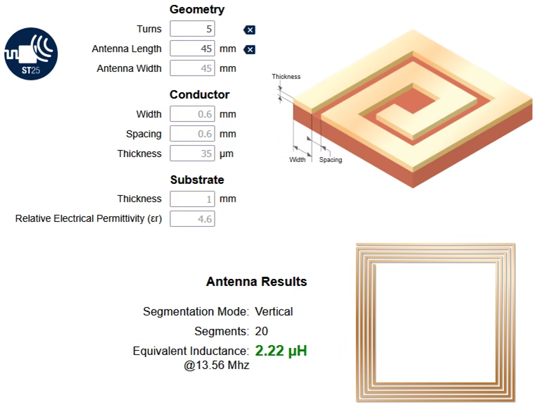
Option 2: (Online) tools
I’ve previously used Cadence Virtuoso to design on-chip inductors, typically around 500 µm in size for LNAs operating at a few GHz. However, an NFC tag requires coils on the order of several tens of millimeters. For this larger scale, a number of dedicated tools are available.
Coil32 (and its successor Coil64) is a free program that calculates inductance, Q, and self-resonance for a wide range of coil types, from air-core solenoids to PCB spirals and ferrite toroids. It runs on Windows, Linux, Mac, and Android, and is popular with hobbyists and RF engineers for quick estimates. While accurate for simple geometries, it cannot fully account for parasitics or complex layouts, so it is best suited for early design stages.
ST’s eDesignSuite offers a dedicated NFC antenna design module. By entering coil parameters such as turns, dimensions, and spacing, it provides estimates of inductance, Q, and resonance specifically tuned for ST’s NFC/RFID chips. It is a convenient starting point for NFC tag or reader antenna design, but its simplified models mean that final designs still require measurement or EM simulation for verification. This method requires you to create an account on ST’s official website.
Option 3: Open Source Antennas
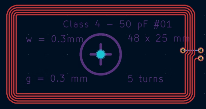
While the first two tools focus mainly on spiral, square, or rectangular coils, it’s worth noting that 90-degree corners are not ideal, just as they are generally avoided in PCB trace design. Designers typically use 45-degree bends or smooth arcs instead. These bends slightly reduce the total trace length of the loop, and therefore the inductance, usually by a small margin. It’s also important to keep the spacing between turns consistent at the bends, which can be tricky to achieve when drawing layouts manually. That is why open-source antenna designs, such as those published by NXP, could simplify your process. They are created with different sizes, but specced to the NXP chips with have a 50 pF internal capacitance.
PCB Business Card
With the basics of NFC covered, we can move on to designing a printed circuit board (PCB) that integrates the antenna, supporting circuitry, and layout. In this section I’ll first walk through the schematic and the choices behind it. After that I present the final PCB design: a business card that incorporates all of these elements.
Schematic
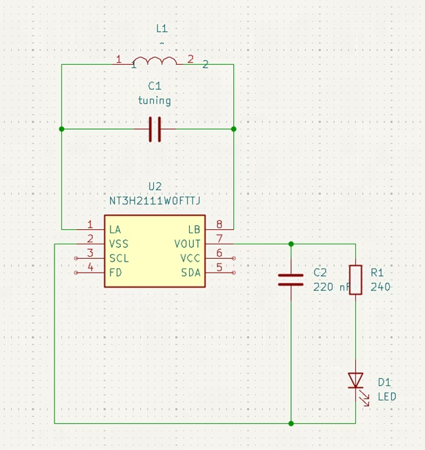
Figure 5 shows the schematic of the circuitry required for operation. At the core is the NT3H2111W0FTTJ IC. On one side, the antenna (L1) is paired with the tuning capacitor (C1), while on the other side the energy harvesting circuitry is connected.
For the antenna, I used the NXP Class 4 design (see Figure 4) as inductor L1. Together with the IC’s internal capacitance (~50 pF) and any external parasitics, the resonance frequency can be further fine-tuned using the tuning capacitor C1. This capacitor is optional and can be soldered in later if adjustment is required.
On the VOUT pin (energy harvesting output), C2 is placed to stabilize the voltage during NFC field modulation or other operating conditions, as recommended by the datasheet. Its value should be between 150 nF and 220 nF. The LED and its series resistor provide a visual indication of harvested power. The resistor R1 is chosen as 240 Ω, which limits the LED current to about 3 mA under typical conditions (see the next section for detailed explanation). A red LED (D1) is chosen because it has the lowest forward voltage (~1.8–2.0 V), so it lights up more reliably at the low voltages available from VOUT. A blue LED (needs ~3 V) would barely light, if at all.
Energy harvesting factor
The energy harvesting behavior of the NT3H2111 requires some additional detail to explain the component choices. Several factors influence how much energy can be harvested from the RF field:
- Antenna size: Larger antennas generally couple more strongly and deliver more energy to the tag
- Turns vs. capacitance: Antennas with fewer turns, combined with an added capacitor to maintain resonance, often provide higher efficiency.
- Field strength: The stronger the reader field, the more energy the tag can harvest.
- Coupling effects: In cases of very strong coupling (large reader coil, very close spacing), the reader itself can be detuned by the tag.
In practice, VOUT will drop under load. If too much current is drawn, the NTAG I²C can no longer maintain RF communication. This point is critical for our design: using a very low series resistor to force ~20 mA into an LED will not work. Instead, the IC current-limits, VOUT collapses, and the supply to the internal circuits may fall below the required VCC, causing the device to stop operating.
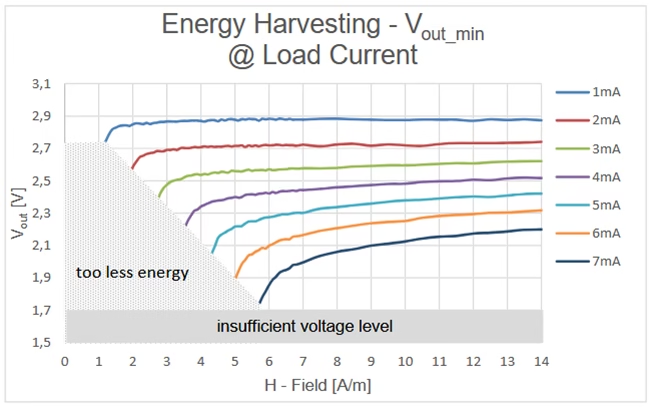
From the NXP application note AN11578, we see that at VOUT ≈ 2.0 V, the available current is limited to about 5 mA. To leave margin, the LED current should be limited to around 3 mA. The same graph shows that at this operating point, VOUT is typically 2.5–2.6 V. With a red LED forward voltage of ~1.8–2.0 V, this leaves ~0.6–0.7 V across the series resistor. The resistor value can then be calculated as:
\[R1 = \frac{0.7\ V}{3\ mA} \approx 233\ \Omega\]
A resistor in the range of 200–240 Ω provides the right balance: the LED is visibly lit (at ~15% of max strength), while current stays within safe limits so the IC can continue to function reliably.
PCB Design
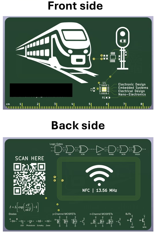
Since I wanted to create a business card, I based the PCB size on a standard bank card: about 85 × 55 mm, with rounded corners. I chose a slightly thinner board (0.6 mm instead of 0.8 mm). This reduced thickness had no cost impact and was still rigid enough to avoid excessive flexing
The overall design is a personal choice, and anyone copying this will probably do it differently. So I’ll just go over the main points and what to watch out for. There are plenty of examples online (1, 2, 3). some even use USB to drive more complex circuits. For me, just having an LED light up through NFC power felt like enough.
Antenna placement is important. Don’t put components or ground planes across the center of the coil area, since that will kill performance. If you really need a ground plane, keep it at least 5 mm away from the antenna edge. The tuning capacitors should sit as close as possible to the IC, while less critical parts like the LED and resistor can live further away.
To check the resonance frequency, the proper tools would be a VNA or a signal generator with an oscilloscope. NXP’sNTAG Antenna Design Guide (AN11276) explains this in detail. I don’t own either, so I’ll just swap around tuning capacitors and see what happens. To make this easier, I added two caps in parallel (both labeled C1). I doubt I nailed it on the first try, so I’ll update once I’ve tested it. And as a side note, if anyone has a spare VNA, free to reach out 😉
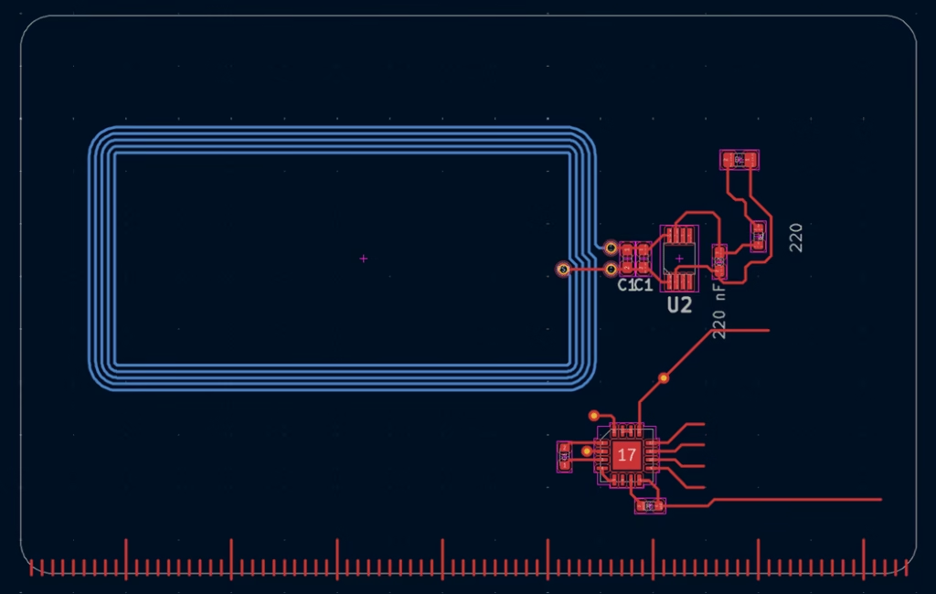
I also added a few dummy footprints to the design, purely for looks with no electrical function. The front and back silkscreen give you plenty of freedom to style the card however you like. Since the PCBs haven’t arrived yet, Figure 8 is just a screenshot from the CAD software. I’ll swap it out for photos of the real boards once they show up.
References
The following links were useful during the design process and may serve as further reading:
[1] NXP Semiconductors. (2018, October 23). NTAG Antenna Design Guide (Application Note AN11276 Rev. 1.8). NXP Semiconductors.
[2] Raziz1. (2025). PCB_Business_Card: A PCB business card with NFC capabilities designed in KiCad [Repository]. GitHub. https://github.com/Raziz1/PCB_Business_Card
[3] NXP Community. (n.d.). NFC discussion forum. NXP. https://community.nxp.com/t5/NFC/bd-p/nfc
[4] STMicroelectronics. (n.d.). M24LR series internal capacitance considerations for antenna tuning (Application Note AN3249). https://www.st.com/resource/en/application_note/an3249-m24lr-series-internal-capacitance-considerations-for-antenna-tuning-stmicroelectronics.pdf
[5] STMicroelectronics. (n.d.). How to design an antenna for dynamic NFC tags (Application Note AN2972). https://www.st.com/resource/en/application_note/an2972-how-to-design-an-antenna-for-dynamic-nfc-tags-stmicroelectronics.pdf
[6] STMicroelectronics. (n.d.). How to design a 13.56 MHz customized antenna for ST25 NFC/RFID tags (Application Note AN2866). https://www.st.com/resource/en/application_note/an2866-how-to-design-a-1356-mhz-customized-antenna-for-st25-nfc–rfid-tags-stmicroelectronics.pdf
[7] STMicroelectronics. (n.d.). NFC Inductance | RF Design | eDesignSuite. STMicroelectronics. Retrieved from https://eds.st.com/antenna/#/
[8] STMicroelectronics. (n.d.). ST25TB04K datasheet. https://www.st.com/resource/en/datasheet/st25tb04k.pdf
[9] NXP Semiconductors. (2023, July 21). NT3H2111_2211 – NTAG I²C plus: NFC Forum T2T with I²C interface, password protection and energy harvesting [Product data sheet]. https://www.nxp.com/docs/en/data-sheet/NT3H2111_2211.pdf
[10] loboat. (n.d.). PCB Business Card With NFC [Instructable]. Instructables. https://www.instructables.com/PCB-Business-Card-With-NFC/
[11] NXP Semiconductors. (2016, February 1). Energy Harvesting with the NTAG I²C and NTAG I²C plus (Application Note AN11578 Rev. 1.0). NXP Semiconductors.
Florius
Hi, welcome to my website. I am writing about my previous studies, work & research related topics and other interests. I hope you enjoy reading it and that you learned something new.
More Posts