

IGBT vs MOSFET: How to Choose the Right Power Switch
This article compares IGBTs and MOSFETs for power electronics applications It covers efficiency trade-offs, conduction and switching losses, voltage/current guidelines, structural differences (such as body diode and tail current), and real-world use-cases like motor drives and inverters Diagrams, formulas, and figures aid understanding for both engineers and enthusiasts.

Sorting Vallejo Paints with Machine Learning
This article explores how to visually sort color collections using both statistics and machine learning. After experimenting with PCA for dimensionality reduction and simple color ordering, I shifted to XGBRanker, a machine learning method that learns personalized color preferences. By comparing these approaches, I aimed to find a method that ...

K-Means Clustering for Colors
Discover how K-Means clustering helps analyze and evaluate Vallejo Model Color paints using Rembrandt’s masterpiece as a case study. Learn to identify gaps in your paint collection and find essential colors for your palette.

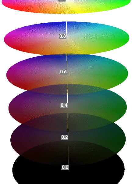
HSV color chart for vallejo paint
Curious how your paints stack up in color space? I analyzed my Vallejo paints by converting RGB values to HSV, visualizing them in 3D, and clustering them to identify dominant groups. Learn how to optimize your miniature paint collection using data-driven insights while keeping your hobby creative and fun.
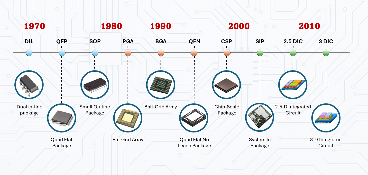
Semiconductor Packaging Technology
Wire bonding and flip-chip packaging represent two fundamental approaches to chip interconnection. While wire bonding offers simplicity and cost benefits, flip-chip allows higher density and faster signals. Adhesive and solder-based methods help balance thermal expansion and reduce stress. The industry continues shifting toward compact, high-performance packaging formats.
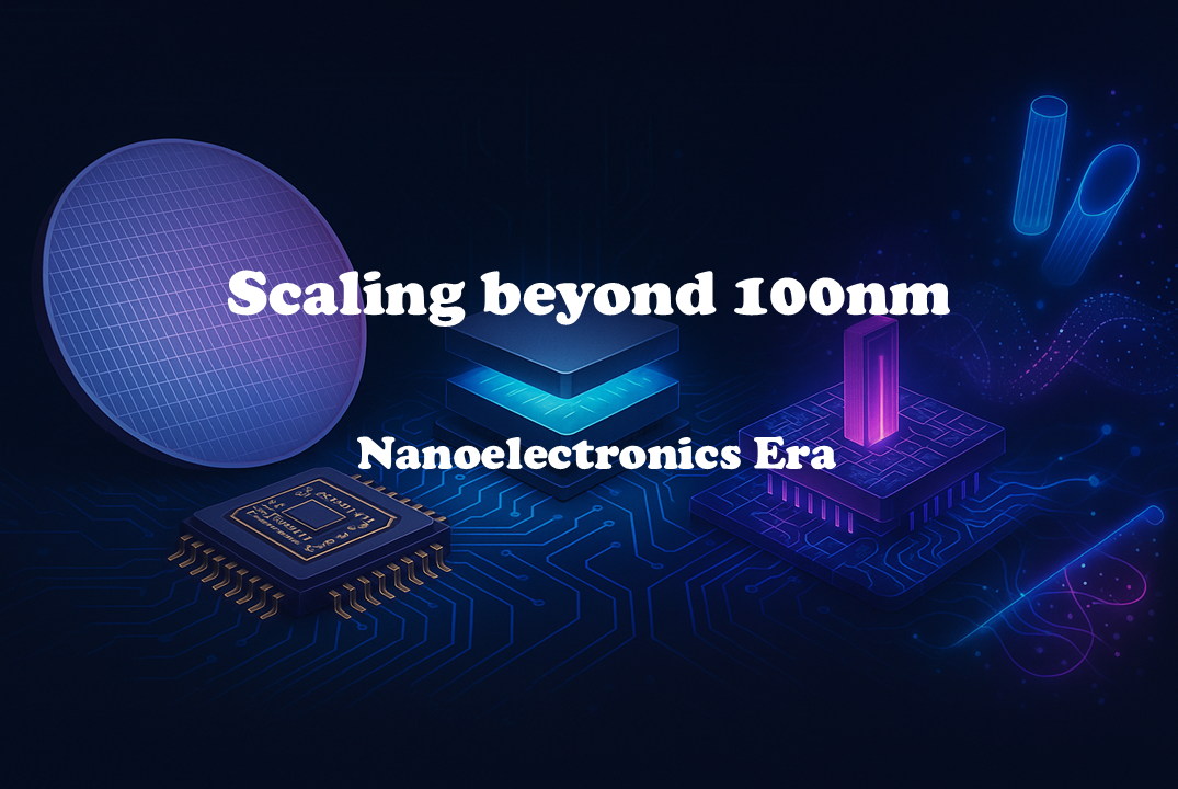
Scaling beyond 100nm – Nanoelectronics Era
As silicon and silicon dioxide reach their scaling limits, engineers turn to high-k materials, metal gates, and new device architectures like FinFETs and SOI. These advances define the nanoelectronics era. Yet even FinFETs have limits—pushing research toward carbon nanotube FETs, tunnel FETs, and spin-based devices that could drive future breakthroughs.
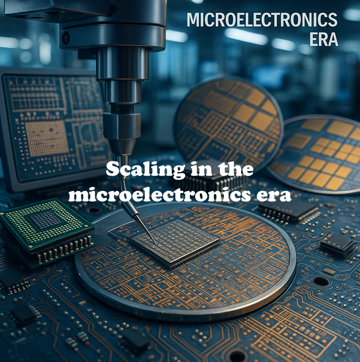
Scaling of CMOS: Microelectronics era
As CMOS technology shrank below 1 μm in the microelectronics era, high electric fields caused reliability issues like hot carrier effects. Techniques such as LATID and Anti-Punch Through (APT) were introduced to control these effects and extend the performance of shrinking devices.
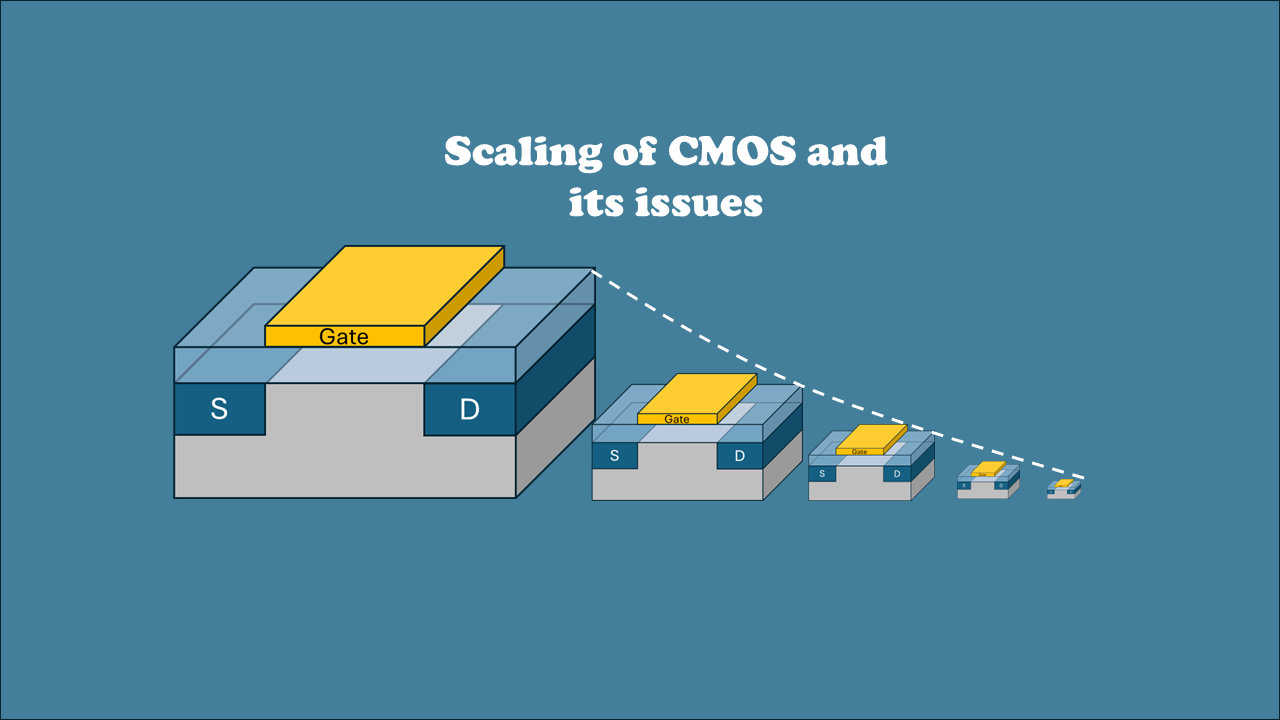
Scaling of CMOS and its Issues
Dennard scaling revolutionized microelectronics by showing that reducing transistor size and voltage proportionally keeps power density constant. However, real-world limitations like subthreshold slope and interconnect resistance eventually halted its ideal progression, demanding alternative approaches to maintain performance improvements in modern technology nodes.
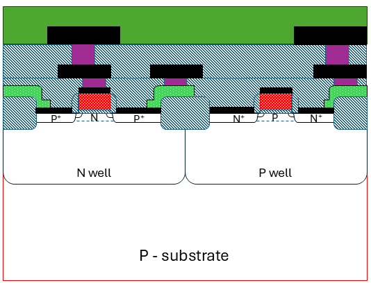
CMOS Process Steps: 3um to 1.25um
CMOS chips are made using a twin-well process, with precise tailoring of each well starting from a lightly doped substrate. Key production steps include using advanced masks, growing silicon oxide and nitride layers, ion implantation for wells, and using the LOCOS technique to isolate chip regions efficiently.
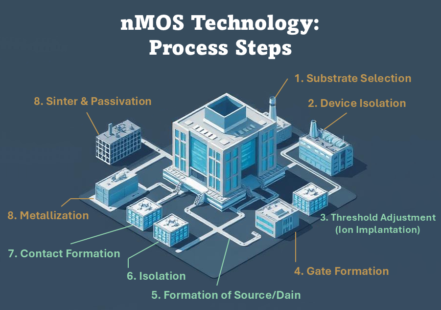
Basic nMOS Technology: Process Steps
NMOS fabrication involves key process steps like substrate selection, isolation, gate formation, and metallization. LOCOS isolation prevents unwanted current flow, while polysilicon gates enhance process stability. Ion implantation controls threshold voltage, ensuring device performance. Learn how NMOS advancements shaped microelectronics until CMOS became the preferred technology.