RSS Daily tech news
  • Chemists set electrons free and break a decades-old chemistry barrier
    Chemists have developed a catalyst that breaks a long-standing rule governing which molecules receive electrons during chemical reactions. By releasing electrons directly into solution, the technique could unlock reactions—and potentially useful new molecules—that were previously out of reach.
  • Scientists just 3D printed one of the hardest metals on Earth
    A new 3D printing technique can produce exceptionally hard tungsten carbide cobalt while using less of its expensive raw materials. By softening rather than fully melting the material, researchers created defect-free samples with industrial-grade hardness and opened the door to more efficient manufacturing.
  • Mysterious Milky Way object accelerates protons beyond one quadrillion electron volts
    Scientists have identified LHAASO J1912+1014u as a cosmic accelerator that can push protons beyond one quadrillion electron volts. The finding may help reveal where the Milky Way’s most energetic cosmic rays come from and how they influence the galaxy.
  • New process turns plastic waste into hydrogen fuel while trapping the carbon
    A new chemical process can transform three of the most common plastics into high-purity hydrogen without sorting them first. The technique operates at much lower temperatures than traditional gasification and captures most of the plastic’s carbon in solid or liquid forms instead of releasing it as carbon dioxide.
  • Scientists built a camera that can track invisible particles in 3D
    A new particle detector called PLATON could replace millions of tiny detector components with a single block of light-producing material. Using a light-field camera, highly sensitive photon sensors, and AI, it reconstructs particle paths in fast, detailed 3D. Simulations suggest it could match or surpass today’s best detectors while being far easier to scale. The […]
  • These tiny holes could change how the world cleans water
    A new nature-inspired membrane uses perfectly uniform one-nanometer pores to filter molecules with remarkable precision. The technology could transform industries such as pharmaceuticals and textiles by reducing energy consumption, improving water reuse, and delivering separation performance far beyond current filters.

Analog layout design rules

by Florius
Featured image of analog layout design rules

Matching transistors layouts is important to minimize variations in electrical characteristics. This is especially true for analog and mixed-signal circuits, such as differential amplifiers, where symmetrical behaviour is critical for high precision and low distortion. Similar to current mirrors, matching transistors ensure accurate current replication, which is critical for biasing and amplification stages. In this article, I will explain several of the important design rules that help in the reduction of mismatch.

1. Same temperature conditions

Let’s start with an obvious (but difficult) layout condition. For optimal matching between two transistors for example, both devices must operate along the same isotherm. Large chips often experience high temperatures, and while silicon is a good thermal conductor, temperature gradients can still arise. For instance, power devices on one side of a chip can create localized heating, affecting other areas.

When power devices heat the chip on the right side, they generate isotherms extending to other regions. Input transistors of an op-amp or differential circuit should ideally be positioned along these isotherms. If not, internal thermal resistance can act like a feedback resistor, limiting the open-loop gain (refer to the source for more details).

The trick with this rule is, is that it can be challenging to find these isotherms.

Fig 1. Keep away from power devices.

2. Current orientation matching

Crystal orientation plays a critical role in achieving good matching in transistors. A crystal’s structure, including properties like density varies depending on direction. Consequently, the mobility μ parameter is not identical in all directions. This phenomenon is highlighted in the following examples:

  • In the first case, current in one transistor flows perpendicular to the current in the other one. This misalignment leads to poor matching.
  • In contrast, the second and third examples show better configurations. While slight variations in source contact resistance may occur due to connection placement, these differences are generally minimal and less impactful.
Fig 2. Orientation is important in analog circuits for matching purposes.

3. Area over perimeter ratio

A highly effective way to improve layout design for better matching is to maintain a consistent area-to-perimeter ratio or use identical shapes for all transistors, ensuring they are the same size. This is because rounding effects on edges and corners have a more pronounced impact on smaller transistors compared to larger ones.

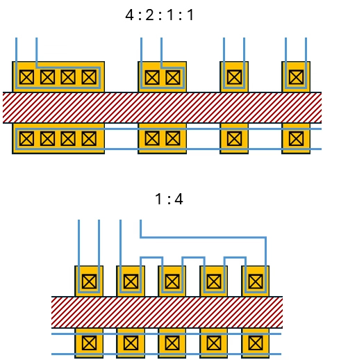
For example, consider the figure below, where the transistor sizes follow relative ratios of 4:2:1:1. These ratios may lack precision because edge rounding disproportionately affects the smaller transistors (size 1) compared to the larger ones (size 4).

A more precise approach involves using identical shapes for all transistors and connecting them in parallel. This method ensures a uniform area-to-perimeter ratio, minimizing the relative impact of local errors. For instance, implementing a 1:4 ratio using this technique yields significantly higher accuracy. While this layout style, common in bipolar transistor designs, requires more space, it greatly improves matching performance. It is generally true that making it bigger improves the matching performance overall.

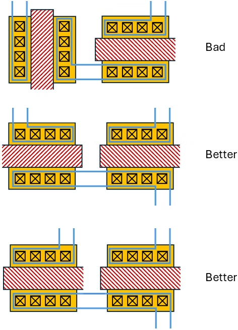
Diagram of two PCB layouts with different fan-out ratios: top layout shows a 4:2:1:1 pattern, bottom layout shows a 1:4 pattern.
Fig 3. Illustration of different via-to-pad routing strategies in PCB layout, showing 4:2:1:1 fan-out on top and 1:4 fan-out on bottom.

4. End dummies

In places with multiple equal structures (such as transistors, capacitors, resistors, etc.), the ones on the outside never match that well. The reason for that is, that these outside structures see different neighbours.  Imagine a 10×10 grid of transistors; all the ones on the inside see transistors all around them, while the outer rim only sees it on the inside and nothing on the outside. Effects of processing, such as etching, contact holes, etc. will be different. That is the reason why dummy structures are placed on the end.

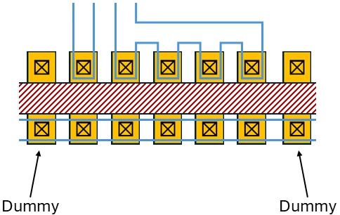
These dummies are not used, and in the case of transistors transistors their VGS = 0. In the figure below you see the example of the previous section with the use of end dummies to improve the performance of all the active transistors. tl;dr, the are only present to make sure that the processes are done homogeneously for all active transistors.

Fig 4. End dummies. Additional structures in analog layout beyond schematic.
Fig 4. End dummies to improve symmetry. Additional structures in analog layout beyond schematic.

5. Centroid layout

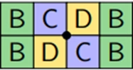
One important layout style to reduce mismatch is the common centroid (CC) layout. In this layout, all segments are placed so that their centroids coincide. For example, the layout in Figure 5 shows a CC layout where the segments C & D have a common centroid marked with the black dot. The segments B on the outer rim could be considered dummies, and can even be extended further to include a top and bottom row. This layout is used in my previous article on how to design an OTA.

Fig 5. Mating technique called Common Centroid
Fig 5. Mating technique called Common Centroid.

The idea behind using CC layouts, is that they cancel out linear systematic variations due to first order process gradients (in oxide thickness, …). Under these assumptions, the CC criterion ensures that the sum of variations over all segments cancel each other out. To get the best out of a CC layout, you want your array to occupy as little space as possible and have a summetry around both x- and y-axis so that the devices are balanced and mirrored both horizontally (x-axis) and vertically (y-axis).

Leave a comment

This site uses Akismet to reduce spam. Learn how your comment data is processed.