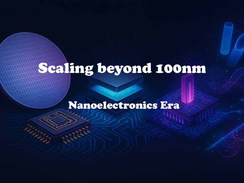

Scaling beyond 100nm – Nanoelectronics Era
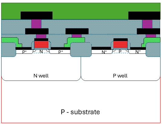
As silicon and silicon dioxide reach their scaling limits, engineers turn to high-k materials, metal gates, and new device architectures like FinFETs and SOI. These advances define the nanoelectronics era. Yet even FinFETs have limits—pushing research toward carbon nanotube FETs, tunnel FETs, and spin-based devices that could drive future breakthroughs.
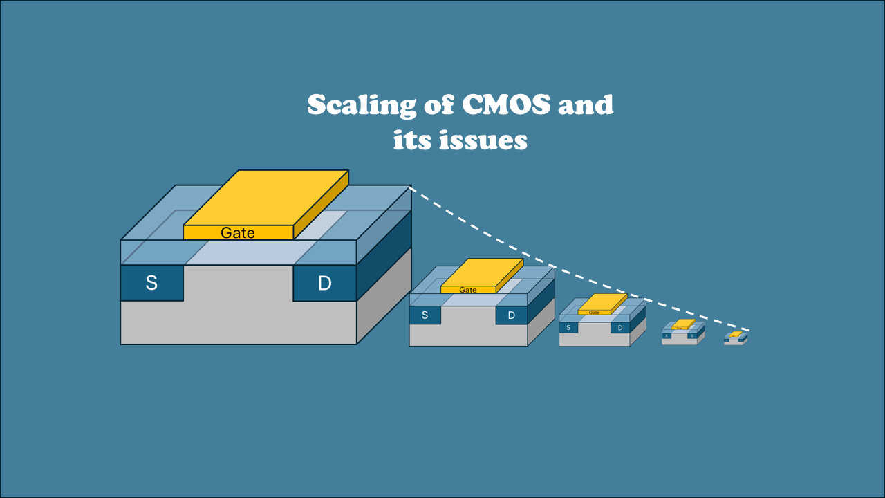
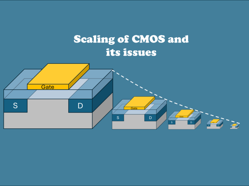
Scaling of CMOS and its Issues
Dennard scaling revolutionized microelectronics by showing that reducing transistor size and voltage proportionally keeps power density constant. However, real-world limitations like subthreshold slope and interconnect resistance eventually halted its ideal progression, demanding alternative approaches to maintain performance improvements in modern technology nodes.