
In this article, we explore the era of nanoelectronics, where device dimensions have scaled from 100 nm down to just a few nanometers. This continues our series on technology of integrated systems, which began with the foundational steps of the NMOS fabrication process. We then examined complementary MOS (CMOS) technology at the micrometer scale. While Dennard scaling allowed continued use of the same materials and techniques, it introduced challenges that became increasingly apparent in the microelectronics era—spanning from 1 μm to 0.1 μm. As you’ll see, at even smaller scales, the conventional MOSFET can no longer meet performance and power demands, prompting the need for new device architectures and innovations.
Table of Contents
We begin this post by acknowledging a key turning point: silicon and silicon dioxide are no longer as effective as they once were. As we approach their physical and performance limits, it’s clear that alternative materials must be considered. However, the primary bottleneck for MOSFET scaling is leakage power, which becomes increasingly problematic at smaller dimensions. To address this, the next major shift involved rethinking the device structure itself. FinFETs emerged as a strong candidate, offering better control over short-channel effects. Yet, at truly nanoscale dimensions, even FinFETs face limitations—leading us to explore Gate-All-Around (GAA) FETs and potentially even carbon nanotube-based transistors or other more advanced technology.
Paradigm shift 1: Introduction of new materials
Silicon and silicon dioxide have long been the foundational materials for transistor technology. Their exceptional properties—particularly the stability of SiO₂ and silicon-based compounds like silicides—enabled the continued miniaturization of transistors. However, further scaling of the SiO₂ gate dielectric thickness eventually stalled due to excessive gate leakage. This led to the adoption of high-k dielectrics to reduce Equivalent Oxide Thickness (EOT) while maintaining gate control. The use of high-k materials, in turn, necessitated the integration of metal gates, often in dual-metal configurations. Even silicon, once considered untouchable, began to show its limits. Alternative channel materials such as germanium and III-V semiconductors were explored due to their superior carrier mobilities [3][4].
Gate insulator scaling
The scaling of the SiO2 layer gives better gate control, thus better switching and faster devices. But at very thin SiO2 layers, below an oxide thickness of tox = 2 mn, the gate leakage current becomes a dominator factor. The reason for this is quantum mechanical tunneling. From equations we can see that the electrical current has the following relation with the thickness of the oxide (L):
\[I(L)\sim P(L) \sim \psi^2(L)\sim e^{-2kL}\sim e^{-2\sqrt{2m\phi / \hbar^2}L}\]

However, the aim is not to have a small tox, but to have a large Cox. Thus the idea is to replace this oxide layer with a thicker high-k material, that has a higher dielectric constant (k), which gives the same or smaller capacitance (and electrical properties) as the thinner SiO2, but with less leakage, because it is physically thicker. This is why we can say that the Equivalent Oxide Thickness is small, even if the physical thickness is not. The Equivalent Oxide Thickness can be calculated by the following formula:
\[\text{EOT} = t_{HK}\frac{k_{SiO_2}}{k_{HK}}\ ,\]
Some of the possible high-k dielectrics included HfO₂, hafnium silicate, Hf–Al–O, and others. Hf-based materials received most of the attention. However, integrating them was not without issues. Silicon tends to oxidize, making it very difficult to avoid the formation of SiO₂ at the interface. Ironically, this issue turned out to be a blessing in disguise: depositing high-k dielectrics directly onto silicon resulted in a much worse interface. A thin interfacial SiO₂ layer between the high-k material and silicon provided a better-quality interface. However, this also limited equivalent oxide thickness (EOT) scaling due to the presence of the SiO₂ layer.
Polycrystalline silicon (poly-Si) gate electrodes are normally doped to behave like metals. However, when interfaced with a high-k dielectric, a depletion region forms in the poly-Si. This reduces the effective gate capacitance, undermining the benefit of using high-k dielectrics. As a result, the industry transitioned back to metal gates. The threshold voltage is now controlled by the work function of the gate metal, requiring different metals for pMOS and nMOS devices.
As you might expect, integrating metal gates is not straightforward. A dummy gate—typically made of poly-Si—is initially used for self-aligning, which is later replaced with a metal having the appropriate work function. In Figure 2, I show the various steps involved in fabricating these metal gates.

Mobility scaling
As gate length scaling slowed due to short-channel effects and the oxide layer was replaced by high-k dielectrics, the next focus became improving carrier mobility (μ):
\[I_d \sim \mu\frac{W}{L}\frac{\varepsilon_{ox}}{t_{ox}}\]
There are three primary strategies to enhance mobility. The first is to induce strain in the channel material. By stretching or compressing the crystal lattice, the unit cell is deformed, which alters the Brillouin zone in k-space. Since the effective mass is related to the curvature of the energy dispersion relation, strain changes the mobility. Several methods exist, including strained silicon on bulk SiGe or applying uniaxial strain through tensile or compressive layers. Tensile strain typically enhances n-MOS performance, while compressive strain benefits p-MOS [2][5].
![Fig 2. Cross sectional SEM of SOI NFET (a), and bulk PFET (b). Image taken from [2].](https://florisera.com/wp-content/uploads/2025/05/strain.avif)
The second strategy is to exploit the mobility dependence on crystal orientation. Different crystal orientations exhibit different periodicities in real and reciprocal space, resulting in varied energy band structures. Consequently, mobility varies with direction. The ⟨100⟩ orientation is favorable for n-FETs, while ⟨110⟩ is preferred for p-FETs.
The third approach involves changing the substrate material. Germanium, for example, exhibits higher carrier mobility than silicon but lacks a stable native oxide like SiO₂. High-k dielectrics can be used to overcome this limitation. However, germanium poses additional challenges—it performs poorly with n⁺ junctions and is thus typically used only for p-MOS devices. This has led to ongoing research into alternative III–V semiconductors, which offer promising mobility characteristics for n-MOS applications [6].
Changing the MOSFET structure
Regardless of the solutions implemented, dynamic power dissipation continued to double approximately every three years, and leakage power also increased significantly. One approach to address this challenge was to optimize MOSFET parameters—such as threshold voltage, oxide thickness, and supply voltage—based on the target application. For example, high-performance logic was used in PCs, low operating power logic in notebooks, and low standby power logic in mobile devices.

By 2006, manufacturers had implemented diverse strategies. AMD, for instance, adopted a triple VT approach: high VT for memory and non-critical circuits to minimize leakage, regular VT for critical paths tuned during manufacturing, and low VT for speed-critical regions where high leakage was tolerated. Intel, on the other hand, favored a single VT strategy to simplify the process and reduce variability. Instead of varying VT, Intel used channel length adjustments—short channels for speed, long channels for leakage control.
You may sometimes hear that turning the device off is more difficult than turning it on. This means that leakage currents (which occur when the device is supposed to be off) are harder to suppress than achieving high current drive when it’s on. All these techniques to boost performance when the device is on, don’t help much with turning it off. If gate control can be improved, turn-off characteristics and short channel effects will also improve. This is what I will try to explain in the next sections.
Paradigm shift 2: Change the device structure
Instead of trying to make the current device work, people were looking at other radical ideas. MOSFET device is a surface device. The bulk of the silicon wafer is not used. You’d like a new structure with better channel control with less vertical parasitics of junctions. Ideally you want to isolate the thin active layer from the bulk. To realize this, a new fabrication method was invented, which is called Silicon On Insulator (SOI).
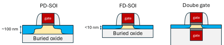
The technique used to place silicon on top of a thick oxide layer is too advanced to cover in detail here. However, SOITEC—the company that manufactures these specialized wafers—offers informative videos on the process, known as SmartCut.
In this article, the focus will be on what can be done with these wafers. Two common types of silicon-on-insulator (SOI) technologies are Partially Depleted (PD) and Fully Depleted (FD) SOI. As the name suggests, in FD-SOI, when a gate voltage is applied, the entire silicon layer under the gate is depleted of free carriers. This provides improved electrostatic control over the channel and reduces short-channel effects, such as threshold voltage roll-off and subthreshold leakage.
An even more advanced variant is the double-gate FD-SOI, also developed by SOITEC. In this structure, a second gate—called the back gate or buried gate—is located beneath the channel. This architecture offers significantly better control over the channel than a single-gate design. However, it presents serious manufacturing challenges, especially regarding alignment and fabrication precision.
This double-gate structure serves as a stepping stone toward the next major architectural evolution in transistor design: the FinFET.
FinFET
The FinFET structure is considered one of the most practical approaches for implementing multi-gate devices with self-aligned gates. As shown in Figure 6, it is a three-dimensional device often built on silicon-on-insulator (SOI) substrates [7].
Notably, in FinFETs, the smallest feature is no longer the channel length, but rather the fin width (Wfin). FinFETs belong to a broader class of devices known as Multi-Gate FETs (MuGFETs). Various FinFET types are illustrated in Figure 6. Today, the tri-gate FinFET is widely used in 10 nm and 7 nm technology nodes. However, the industry is now transitioning toward Gate-All-Around (GAA) FinFETs for even smaller nodes (e.g., 3 nm and below), as they offer superior electrostatic control.
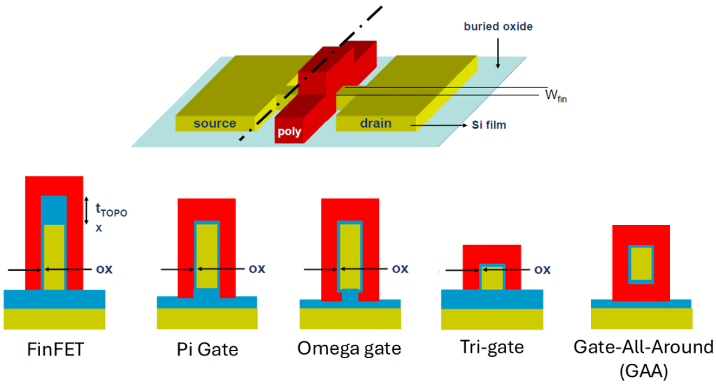
As stated in the ITRS 2005 roadmap, the width of the fin (Wfin), is the most crucial parameter, not Lg. In the end, this type of MOSFETs, also have their own issues, such as the orientation of the silicon crystal structure in the fins (as discussed before), or the doping of these fins. As shown in the Figure 7, the threshold voltage is very sensitive to the thickness of the fin when it is doped.

New (nano) Devices
While silicon-based MOSFET scaling continues below the 10 nm mark, researchers are already exploring technologies that could extend the semiconductor roadmap beyond traditional scaling. Promising candidates include semiconductor nanowires, carbon nanotubes, and steep-subthreshold-slope devices such as tunnel FETs and ferroelectric FETs. Even more revolutionary concepts are being investigated, including spin-based devices like skyrmion racetrack memory and spin-transfer torque (STT) RAM. This evolution highlights the growing convergence of biology, chemistry, and physics with electronics—paving the way for a new era of nanotechnology [8][9].
![Fig 7. An STT-RAM cell (left), and double-gate CNFET (right). Images were taken from [8][9].](https://florisera.com/wp-content/uploads/2025/05/new-devices-768x309.png)
References
[1] Internet website: http://ixbtlabs.com/articles2/intel-65nm/indexOLD.html
[2] C. D. Sheraw, et al., Dual Stress Liner Enhancement in Hybrid Orientation Technology, Symposium on VLSI Technology Digest of Technical Papers, 2005.
[3] G. Dewey, et al., Logic performance evaluation and transport physics of Schottky-gate III–V compound semiconductor quantum well field effect transistors for power supply voltages (VCC) ranging from 0.5v to 1.0v,IEEE International Electron Devices Meeting (IEDM), 2009.
[4] H.Y. Yu, et al, High performance n-MOSFETs with novel source/drain on selectively grown Ge on Si for monolithic integration, IEEE International Electron Devices Meeting (IEDM), 2009.
[5] C. Auth, et al., 45nm High-k + metal gate strain-enhanced transistors, Symposium on VLSI Technology, 2008.
[6] C.O. Chui, and K.C. Saraswat, Advanced Germanium MOS Devices and Technology, IEEE Conference on Electron Devices and Solid-State Circuits, 2005.
[7] M.G.C. Andrade, and J.A. Martino, Threshold voltages of SOI MuGFETs, Solid-State Electronics, 2008.
[8] S.M. Seyedzadeh, et al., Leveraging ECC to Mitigate Read Disturbance, False Reads and Write Faults in STT-RAM, 46th Annual IEEE/IFIP International Conference on Dependable Systems and Networks, 2016.
[9] Y.M. Lin, et al., High-Performance Carbon Nanotube Field-Effect Transistor With Tunable Polarities, Appl. Phys. Lett. 73, 2447–2449 (1998).
Further reading:
IEEE Distinguished Lecture Series, Friday, April 1 st, 2005 CMOS. Scaling Limits and Nanoelectronic Devices, by Yoshio Nishi.
Florius
Hi, welcome to my website. I am writing about my previous studies, work & research related topics and other interests. I hope you enjoy reading it and that you learned something new.
More Posts