A groundbreaking collaboration between Los Alamos scientists and Duke University has resurrected a nearly forgotten 1938 experiment that may have quietly sparked the age of fusion energy. Arthur Ruhlig, a little-known physicist, first observed signs of deuterium-tritium (DT) fusion nearly a decade before its significance became clear in nuclear science. The modern team not only […]
At Flinders University, scientists have cracked a cleaner and greener way to extract gold—not just from ore, but also from our mounting piles of e-waste. By using a compound normally found in pool disinfectants and a novel polymer that can be reused, the method avoids toxic chemicals like mercury and cyanide. It even works on […]
Imagine detecting a single trillionth of a gram of a molecule—like an amino acid—using just electricity and a chip smaller than your fingernail. That’s the power of a new quantum-enabled biosensor developed at EPFL. Ditching bulky lasers, it taps into the strange world of quantum tunneling, where electrons sneak through barriers and release light in […]
Harvard and PSI scientists have managed to freeze normally fleeting quantum states in time, creating a pathway to control them using pure electronic tricks and laser precision.
Electronics often get thrown away after use because recycling them requires extensive work for little payoff. Researchers have now found a way to change the game.
Physicists have developed a lens with 'magic' properties. Ultra-thin, it can transform infrared light into visible light by halving the wavelength of incident light.
This article delves into the fundamental properties and diverse applications of metals, covering everything from their atomic structure and conductivity to their critical role in modern technology. In this post, I will focus on the conductivity of metals, exploring the various models developed to explain this phenomenon. Once we have a solid understanding, I’ll discuss how resistivity is further influenced by scattering phenomena. There are many more fascinating aspects of metals to explore, such as transparent metals and advanced conductors, which will be covered in my upcoming post. Stay tuned for more!
1. Introduction into Conductivity of Metals
One of the important properties of metals is that they have high conductivity. These solids have a partially filled upper energy band. When an electric field is applied to the material, electrons can be easily excited toward upper energy levels within the same band, where they become “quasi” free to move in the electric field, giving rise to a low resistivity. In certain metals, like Mg, the valence band is filled, but there is an overlap with the conduction band, such that the energy gap EG=0 . We can divide materials depending on their energy gap in three different categories:
Metals (overlapping bands or single band)
Semiconductors (~0.7 eV till 3.5 eV)
Insulators (> 4 eV)
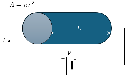
A fundamental equation pertaining to electrical conduction of materials is Ohm’s law, which has been extracted from experimental observations.
\[
R= \frac{V}{I}
\]
The resistance R is proportional to the length L of the sample and inverse proportional to the cross-sectional area A, so that R=ρL/A, where ρ is a material parameter, i.e. specific resistivity (in Ohm-m).
Fig 1. Ohm's law.
However, in scientific literature (and in this article) we normally use a different form, because it is independent on the sample’s dimension. In a uniform sample, the electric field is given by E=V/L, and the current density is J=I/A. As such, the materials scientist’s version of Ohm’s law becomes:
\begin{equation}
J=\sigma E,
\end{equation}
where σ=1/ρ is the electrical conductivity. It expresses a relation that is valid locally at every point in the material. It is a relation showing the two vector quantitites, the electric field E and the current density J, are parallel and proportional everywhere in the material. Keep in mind that for anisotropic materials, conductivity is not a simple scalar, but is a nine-component tensor.
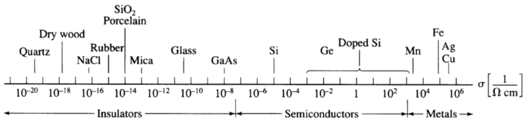
The conductivity σ of different materials spans about 25 orders of magnitude. One of the largest known variation in a physical property.
Fig 2. Room-temperature conductivity of various materials. (Superconductors, having conductivities of many orders of magnitude larger than copper, near 0 K, are nto shown. The conductivity of semiconductors varies substantially with temperature and purity).
A satisfactory understanding of electrical phenomena on an atomistic basis was achieved by Drude. The understanding was later refined by quantum mechanics in the Sommerfeld model.
2. Classical approach (Drude model)
Drude assumed that many electrons are available in states very close to empty states and that they behave like a free-electron gas. He proposed that all these electrons are free to move. Drawing an analogy to gas kinetics, he assumed that the average kinetic energy mv2/2 of the electrons was kBT/2 per degree of freedom, or 3kBT/2 in a three-dimensional free-electron “gas.” Using this analogy, he calculated the velocity. From the equations mentioned, he derived the thermal velocity vthas:
\[
v_{th} = \sqrt{\frac{3k_BT}{m}},
\]
where kB is the Boltzmann’s constant and m the electron mass. At a temperature of 300 K, he predicted vth =105 m/s. He interpreted this as the velocity an electron acquires from thermal energy, representing the average speed of electrons inside the metal. However, since electrons move randomly in all directions, their individual velocities cancel each other out, resulting in no net motion. Nevertheless, this calculation provides insight into the high-speed, random motion of electrons in the metal.
2.1 Drift velocity of electrons
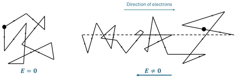
When an electric field E is applied, the free-electron gas develops an average drift velocity (vD) in addition to its random thermal velocity. This drift velocity pushes the electrons in a specific direction as is show in Figure 3. It is the drift velocity that determines the electric current, which can be expressed as:
\begin{equation}
J = -eN_ev_D,
\end{equation}
where e is the charge of an electron, Ne is the number of carriers, and vD is the average drift velocity.
Fig 3. Without an electric field, the individual velocities cancel out. Applying an electric field, will create a net drift of electrons.
If Ne is independent of E, Ohm’s law is satisfied, provided the drift velocity is proportional to the electric field. This proportionality constant in this relationship is known as the mobility of free electrons, μe, which links vD and E through the equation:
\begin{equation}
v_D = -\mu_eE,
\end{equation}
where the negative sign indicates that electrons move in the direction opposite to the electric field. The conductivity is then given by combining equations (1)(2) and (3), to get the following:
If the electrons are accelerated by a force eE, as shown in Figure 3, a net drift of electrons can be expressed by Newton’s law (F=ma):
\[
m\frac{dv}{dt} = eE
\]
where m is their mass and dv/dt is the acceleration. If the electrons were totally free, (such as in vacuum), this constant acceleration would lead to a steadily increasing velocity, and the electron would gain more and more kinetic energy from the field.
However, in the metal, the free electrons are interacting with the lattice ions, as illustrated in Figure 4 (a). Taking this interaction into account, the above equation can be modified as by adding an additional damping term:
\[
m\frac{dv}{dt}+\gamma v = eE
\]
The second term in this equation is a damping or friction force. The electrons are thought to be accelerated until a final drift velocity, vf, is reached (Figure 4 (b)). At that time, the electric field force and the friction force are equal in magnitude. For the steady state case v=vf, we obtain dv/dt=0. The previous equation than reduces to γvf = eE which yields γ = eE/vf.
Fig 4. (a) Schematic representation of an electron path through a conductor containing impurities and grain boundaries, under the influence of an electric field. (b) Velocity distribution of electrons due to the force and counteracting friction force. The electron reaches a steady state final velocity vf. This image was taken from [1].
The complete equation for drifting electrons under the influence of an electric field becomes:
Note that the factor mvf/eE has a unit of time, which is sometimes denoted as τ, the relaxation time. This can be interpreted as the average time between two consecutive collisions. From this we obtain vf=τeE/m, filling this result in equations (1) and (2), J=eNevf=σ. The equation for conductivity becomes:
\[
\sigma=\frac{N_ee^2\tau}{m}
\]
This teaches us that the conductivity is large for materials with a large number of free electrons and a large relaxation time. The latter is proportional to the mean free path (l=vfτ) between two consecutive collisions. This can become important when we have nanoscale structures, where the mean free path might be of the same order than the typical dimensions of the structure itself. Interesting things can happen, such as ballistic transport. Note that in the model of Drude, all the electrons contribute to the conductivity, which is incorrect. In the next model, we will incorporate quantum mechanics to get better approximations.
Sommerfeld realized that not all electrons in a metal contribute equally to electrical conduction. Instead, only the electrons occupying the highest energy levels determine the material’s conduction properties.
In this model, it is assumed that when an electric field is applied to a metal, the electrons at the highest occupied energy level, the Fermi energy (EF), are excited to higher energy states and behave as “quasi-free” electrons. These are the electrons that participate in electrical conduction.
From quantum mechanics, electrons in a solid fill energy bands, with a maximum of two electrons per energy level, as required by the Pauli exclusion principle. For metals at absolute zero temperature (T = 0 K), the highest occupied energy level is the Fermi level, which is different from the Fermi level in semiconductors.
In metals, the Fermi level corresponds to the energy at which the electron states are filled up to at T = 0 K, and it lies within a partially filled conduction band.
In semiconductors, the Fermi level typically lies within the bandgap, midway between the conduction and valence bands (at intrinsic equilibrium).
The Fermi level in metals is given by:
This velocity arises from quantum mechanical considerations and differs from thermal velocity. The Fermi velocity provides a more precise measure of electron dynamics in a metal.
This velocity arises from quantum mechanical considerations and differs from thermal velocity. The Fermi velocity provides a more precise measure of electron dynamics in a metal.
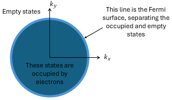
3.1 Fermi Sphere and Occupied States
at T = 0 K, the electron distribution in k-space (momentum space, where p=hk), can be represented as a Fermi sphere (see Figure 5).
All points inside the Fermi sphere correspond to occupied electron states.
The surface of the sphere, called the Fermi surface, represents states at the Fermi energy and separates occupied states from empty ones.
When no electric field is applied, the net momentum of electrons is zero. For every state with wave vector k, there exists a corresponding state with wave vector -k, leading to a net zero balance in momentum.
Fig 5. Fermi sphere in k-space. Inside the sphere, all states are occupied with electrons, while outside of the sphere they are empty. The light blue edge indicates the line between at the Fermi level, separating these two regions.
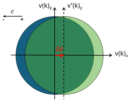
When an electric field is applied, the Fermi sphere shifts in k-space by an amount δk. This causes electrons near the Fermi energy to acquire a net momentum, resulting in a current within the material. In velocity space (directly related to k), this shift causes an asymmetry. Figure 6 illustrates this behavior; when an electric field is applied, the Fermi sphere is displaced. The light green region on the far right remains uncompensated, giving the electrons a net momentum (and velocity) and driving conduction.
This shows the clear difference between the Drude model and the Sommerfeld model, as only the electrons close to the edge contribute to the mobility. Furthermore, only a little extra energy EF is needed to raise a substantial number of electrons from the Fermi level into slightly higher states. As a consequence, the energy (or the velocity) of electrons accelerated by the electric field ε is only slightly larger than the Fermi energy EF (or the Fermi velocity vF) so that for all practical purposes, the mean velocity can be approximated by the Fermi velocity.
Fig 6. Velocity of electrons in two-dimensional velocity space when an electric field is applied which. The shift is indicated by the red arrow.
3.2 Theoretical calculation of the conductivity
The displacement Δk of the Fermi sphere in k-space under the unfluence of an electric field can be calculated by:
We know that the $E(k)$ relationship for free electrons is given by: $E=\frac{\hbar^2 k^2}{2m}$. We can than approximate it further, by saynig that for $k$ near $k_F$ (the Fermi wave vector: $\frac{dE}{dk} \approx \frac{\hbar^2 k_F}{m}=\hbar v_F$.
where ε is the applied electric field. This yields:
\[
dk=\frac{e\varepsilon}{\hbar}dt \text{ or } \Delta k=\frac{e\varepsilon}{\hbar}\Delta t=\frac{e\varepsilon}{\hbar}\tau
\]
where τ is the time interval Δt between two collisions or the relaxation time. From here we can calculate the current density J by following the next approach.
\[
J=ev_FN^*
\]
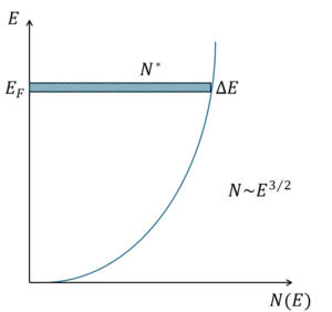
where N* is the number of electrons displaced by the electric field: N* = N(E)ΔE. This results in:
\[
J=ev_FN(E)\Delta E = ev_FN(E)\frac{dE}{dk}\Delta k
\]
We know that the E(k) relationship for free electrons is given by: E=h2k2/2m. We can than approximate it further, by saying that for k near kF (the Fermi wave vector):
Fig 7. Showing the energy vs concentration of electrons. The number of electrons displaced by the electric field is marked as N*. This happens at the Fermi energy level.
By fillling these results into the equation for the current, we obtain:
\[
J=e^2v_F^2N(E)\varepsilon\tau
\]
This Figure further tells us why metals are much more conductive than semiconductors. The density of states, and the amount of electrons avaialble is very high close to the fermi level for metals. This is ofcourse in combination with a low relaxation time.
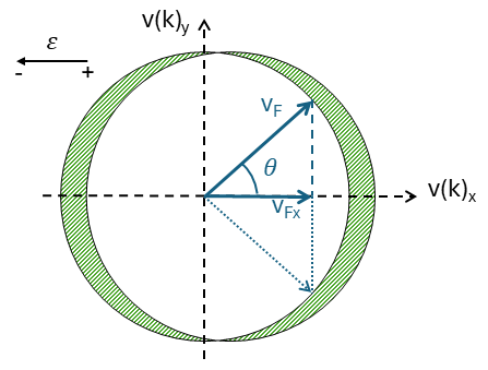
There is more issue that needs to be corrected. When applying a field in one direction (i.e. along negative v(k)x), then only the components of the velocities which are parallel to the positive v(k)x direction contribute to the electric current. The v(k)y components cancel each other out. To accuount for that, we can sum up all the contributions of the velocities in the 1st and 4th quadrant (of Figure 8), which yields:
For a 3D spherical Fermi surface, the calculation yields:
\[
J=\frac{1}{3}e^2N(E)\varepsilon\tau v_F^2
\]
thus the conducitivity finally becomes (with σ=J/ε):
\[
\sigma=\frac{1}{3}e^2N(E)\tau v_F^2
\]
This quantum mechanical equation reveals that the conductivity depends on the Fermi velocity, the relaxation time and the population density. The latter is as we know proportional to the density of states. This equation is more meaningful than the expression derived from the classical electron theory. Since it contains the information that not all free electrons are responsible for conduction, that is the conductivity in metals depends to a large extent on the population density near the Fermi surface.
3.3 Metal energy bands
The Sommerfeld model provides insights into the differences in electrical conductivity between monovalent metals (e.g., copper, silver, gold) and bivalent metals (e.g., magnesium, calcium, zinc). For monovalent metals, the Fermi level is typically located at an energy level with a higher density of states, Z(E), which enhances conductivity.
In Figure X:
Panel (a) shows diamond as an insulator, where the Fermi level lies in the middle of the bandgap.
Panel (b) depicts a metal such as copper, silver, or gold, where the Fermi level is positioned within a partially filled band, resulting in a high density of conduction electrons and excellent conductivity.
Panel (c) illustrates the case of overlapping bands, as seen in magnesium, where the Fermi level lies near the top of the 3s band and the bottom of the 3p band. This region has a lower density of states, leading to reduced conductivity compared to alkali metals.
Fig 9. Schematic represenation of the density of states. Examples for (a) a diamond, (b) Alkali metals and (c) magnesium. The energy levels are indicated by Ei (insulator), Em (monovalent) and Eb (bivalent) metal. This figure was taken from [1].
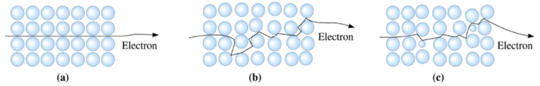
4. Resistivity and Scattering Phenomenas
Conductivity is determined not only by the density of states but also by the relaxation time , which represents the time between two collisions of an electron. τ can have a significant effect on conductivity. In this section, we focus on resistivity (ρ), which is the inverse of conductivity. Relaxation time is closely tied to electron scattering phenomena: the more scattering events, the shorter τ. Two major scattering mechanisms are commonly observed in solids, as shown in Fig. 10:
Fig 10. Movement of an electron through (a) a perfect crystal, (b) a crystal heated to a high temperature, and (c) a crystal containing atomic level defects
(a) A perfect crystal: In an ideal crystal, electrons move uninterruptedly without scattering.
(b) A heated crystal: When the crystal is heated, the atoms vibrate due to thermal energy, creating lattice vibrations known as phonons. Phonons increase the probability of electron-atom collisions, which shortens the relaxation time and reduces the mean free path of electrons. Consequently, conductivity decreases, and resistivity increases with temperature in metals.
For semiconductors, the situation is different. Conductivity increases with rising temperature because thermal energy excites more electrons into the conduction band. This difference provides a simple way to distinguish between metals and semiconductors: by heating the material and observing how resistivity changes.
The increase in resistivity caused by heating metals poses challenges in microelectronics. Copper interconnects and lines, for instance, suffer from higher resistivity at elevated temperatures. During device fabrication, high temperatures are often required, which further exacerbates the issue. At operating temperatures, this higher resistivity leads to greater energy loss, increased heating of the interconnects, and reduced energy efficiency.
(c) Impurities in the crystal: The presence of impurities in the system also increases resistivity. Impurities act as scattering centers, disrupting the movement of electrons. Therefore, the purer the metal or crystal structure, the better the conductivity.
4.1 Mathiessen's rule
The rates of these collisions are often independent to a good approximation, so that if the electric field were switched off, the momentum distribution would relax back to its ground state with a net relaxation time:
where τL and τi are the collision times for scattering by phonons and by imperfections respectively. The net resistivity is give by ρ = ρL + ρi. In general ρL is independent of the number of defects when the concentration is small, and ρi is independent of temperature. This empirical observation expresses Mathiessen’s rule. According to this rule, resistivity arises from independent scattering processes which are additive.
4.2 Resistivity of alloys
Solute atoms are the atoms of an element that are dissolved in a base metal (called the solvent) to form an alloy. The solute atoms are usually different in size, charge, or electronic structure compared to the solvent atoms, which can cause disturbances in the metal’s lattice structure.
For example:
In brass, zinc atoms (solute) are dissolved in copper (solvent).
In steel, carbon atoms (solute) are dissolved in iron (solvent).
These solute atoms often act as impurities and can affect properties like conductivity, strength, and resistivity by interacting with the host metal’s electrons and lattice.
When solute atoms are not randomly distributed and instead form an ordered arrangement within the matrix, the electrons are scattered coherently. This ordering reduces the resistivity of the alloy.
An example of this behavior can be observed in certain Cu-Au alloys, where appropriate processing, such as optimized annealing, leads to the periodic arrangement of solute atoms, enhancing the alloy’s electrical properties.
Fig 11. Schematic represenation of the resistivity of ordered and disordered copper-gold alloys. Image taken from [1].
5. References
[1] Hummel, R.E. (2011). Electrical Conduction in Metals and Alloys. In: Electronic Properties of Materials. Springer, New York, NY. https://doi.org/10.1007/978-1-4419-8164-6_7
Hi, welcome to my website. I am writing about my previous studies, work & research related topics and other interests. I hope you enjoy reading it and that you learned something new.
![Fig 4. (a) Schematic representation of an electron path through a conductor containing impurities and grain boundaries, under the influence of an electric field. (b) Velocity distribution of electrons due to the force and counteracting friction force. The electron reaches a steady state final velocity vf. This image was taken from [1].](https://florisera.com/wp-content/uploads/2025/01/Final-drift-velocity-768x247.png)
![Fig 9. Schematic represenation of the density of states. Examples for (a) a diamond, (b) Alkali metals and (c) magnesium. The energy levels are indicated by Ei (insulator), Em (monovalent) and Eb (bivalent) metal. This figure was taken from [1].](https://florisera.com/wp-content/uploads/2025/01/Monovalent-vs-bivalent-metals-768x306.png)
![Fig 11. Schematic represenation of the resistivity of ordered and disordered copper-gold alloys. Image taken from [1].](https://florisera.com/wp-content/uploads/2025/01/Alloys-768x218.png)