

1. Introduction
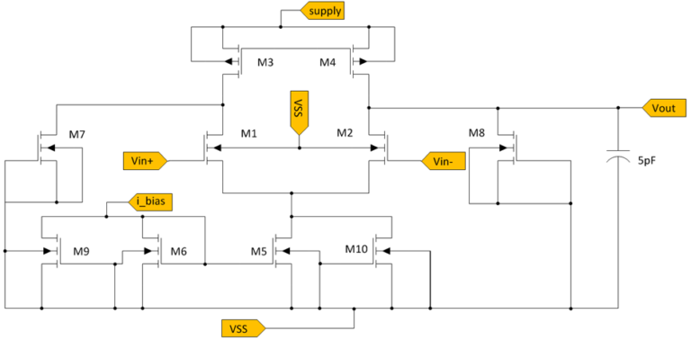
In this article, I will explain how to design an Operational Transconductance Amplifier (OTA) in Cadence, focusing on the techniques and methods used to determine the optimal dimensions of the transistors. We will start with a simple one-stage OTA circuit, as shown in Figure 1, and develop its schematic into a complete layout.
An OTA is an electronic amplifier that generates an output current proportional to the input voltage difference. Essentially, it acts as a voltage-to-current amplifier, converting input voltage signals into output current signals.
The goal of this design is to create a layout for the OTA with a small footprint, meaning the width and length of the transistors should be as small as possible. I will show two different calculation methods. First, hand calculations will provide initial insights into the transistor dimensions. The gm/ID tool in Cadence will offer a more realistic model for further refinement. Using these results, along with additional simulations, you can accurately determine key performance parameters such as gain, bandwidth (BW), and gain-bandwidth product (GBW).

In typical circuit design, you must meet specific performance requirements based on the overall system’s needs. For this example, let’s assume the specifications listed in Table 1 must be achieved. On the left side of the table are the design specifications, while on the right are the technical parameters provided by the IC foundry.
It is important to note that the oxide capacitance differs between nMOS and pMOS transistors due to variations in carrier mobility. Similarly, the threshold voltage is not the same for the two transistor types. These differences must be considered during the design process.
| Specifications | nMOS | pMOS | |||
| CL | 5 pF | μCox/2 | 289 μA/V2 | 54 μA/V2 | |
| Ibias,max | 500 μA | Vth | 0.528 V | 0.491 V | |
| Av | 36 dB | VE | 20 V/μm | 20 V/μm | |
| BW | 1 × 10⁶ Hz | VDD | 1.8 V | 1.8 V | |
| L (min) | 180 nm |
2. Hand calculations
The parameters of interest in transistor design are the width (W) and length (L) of the transistors. In this exercise, we will use sizes in the micrometer (μm) range. Designs at 5 nm or 7 nm scales are beyond the scope of this article, as they delve more into the realm of physics than traditional electronics, involving effects such as quantum tunneling. Furthermore, those names are more marketing terms than actual transistor dimensions, but that is beyond our focus here.
To estimate performance parameters, a “back-of-the-envelope” calculation can provide insights into the trends and trade-offs in the design process. For a first approximation, all transistors are assumed to operate in the saturation region, with (VGS – Vth) = 0.2 V. The two key equations used to calculate the width and length are:
\[\frac{W}{L} = I_{DS}\times\frac{2}{\mu\times C_{ox}}\times\frac{1}{(V_{GS}-V_{th})^2}\]
\[L_{nMOS} = L_{pMOS} = \frac{r_{DS}\times I_{DS}}{V_E}\]
The small-signal output resistance, rDS , is defined as rDS = 1/gDS where gDS is the small-signal conductance. VE the Early Voltage, also plays a crucial role in determining rDS.
Our initial assumption is that rDS is identical for both nMOS and pMOS transistors, which implies that LnMOS =LpMOS . Based on this assumption, we proceed to calculate IDW and rDS as shown in the next sections
2.1 Calculate the Gain-Bandwidth and Transconductance
First, we calculate the Gain-Bandwidth (GBW) and the transconductance (gm). The transconductance measures the transistor’s ability to convert small changes in input voltage into proportional changes in output current. The calculations are performed using the following steps:
\[20\times \text{log}|A_v| \rightarrow |A_v|=63.1\]
\[GBW = |A_v|\times BW = 63.1 MHz\]
The transconductance of the input pair, gm, is calculated using the formula:
\[g_m= GBW\times (2\pi C_{out})\]
where Cout = CL + Cparasitic. For simplicity, parasitic capacitance is neglected, and we assume Cout = CL = 5 pF. Substituting these values:
\[g_m = 1.98\times 10^{-3} \frac{F}{s}\]
2.2 Calculating the output resistance
Since the transconductance gm converts input voltage to output current, and the gain represents the proportionality between input and output voltages, the output resistance, Rout, can be determined as:
\[R_{out} = \frac{A_v}{g_{m1}} \approx 31.83 k\Omega\]
Next, we calculate the small-signal output resistance (rDS) for transistors M2 and M4. For simplification, we assume rds2 and rds4. Using the equivalent circuit, which models these resistances as a parallel connection, the output resistance is:
\[R_{out} = \frac{r_{ds2}\times r_{ds4}}{r_{ds2}+r_{ds4}}\]
Since rds2 = rds4, we solve for rds2 as follows:
\[r_{ds2}=r_{ds4}=2\times R_{out} = 63.67 k\Omega\]
2.3 Calculating current through current mirror
To calculate the current through the left and right branches of the current mirror, we assume that the input pair transistors operate in the saturation region with VGS – Vth =0.2 V. The current is then given by:
\[I_{DS} = \frac{g_{m1}\times(V_{GS}-V_{th})}{2} = 198 \mu A\]
2.4 Calculated dimensions
Using the previously calculated parameters, we can determine the W/L ratios for the nMOS and pMOS transistors. The results are:
- for nMOS: W/L = 17.15
- for pMOS: W/L = 91.77
Having only the W/L ratio is insufficient. The length must be calculated separately.
\[L_{nMOS}=L_{pMOS}=\frac{r_{DS}\times I_{DS}}{V_E}=\frac{I_{DS}}{g_{DS}V_E}=0.637 \mu m\]
Therefore, the width of M2 and M4 can now be calculated to be:
- WnMOS = 10.81 μm
- WpMOS = 57.84 μm
While precise calculations for transistors M5 and M6 are not provided, a logical assumption can be made. Since the current through these transistors is twice that of other nMOS transistors, doubling their width is reasonable. Additionally, to improve matching in the current mirror, increasing the length helps mitigate variations and enhances performance. With that, the final summary of all transistors is shown in the following table.
| M1 | M2 | M3 | M4 | M5 | M6 | |
| W | 11 μm | 11 μm | 58 μm | 58 μm | 22 μm | 22 μm |
| L | 637 nm | 637 nm | 637 nm | 637 nm | 2 μm | 2 μm |
The maximum bias current is limited at 500 µA and because this current is split over two paths, each transistor will only see half of the maximum current. With and , this will result in Of course, this will be in the extreme case where the current through the transistors mirrors the bias current perfectly. To allow for some margin, it is assumed that the transistor current will be 200 µA instead (for transistors M1 to M4 each) and a total of 400 µA (for transistor M5). This would give a starting point.
3. gm/ID methodology
A more precise method is to use the gm/ID methodology in Cadence, which involves performing a transistor DC sweep using models identical to those used in simulation. The tool “gmID” generates several graphs, two of which are most critical for calculating transistor dimensions. The first is the Gain vs. gm/ID graph, as shown in Figure 2. This graph plots the gain (gm/gDS) against gm/ID, indicating the minimum transistor length (L) required to achieve a specific gain. Key observations from this graph include:
- Increasing L enhances the transistor’s gain. This aligns with the equation gDS =IDS / LVE , where a larger L reduces gDS , resulting in a higher gain.
- Low gm/ID indicates velocity saturation, which correlates with reduced gain (see Figure 2).
- Higher gm/ID shifts the transistor into weak inversion, beneficial for lowering power consumption.

From our hand calculations, we know the gain equals 127. Figure 2 demonstrates that only a transistor length of 720 nm or 1 µm meets this criterion at a gm/ID of 10. Transitioning into weak inversion can achieve a sufficiently high gain to allow the use of smaller lengths; however, this comes at the cost of increased transistor width, as shown later.
The second crucial graph, not shown here, is the ID/W plot, which provides the data needed to calculate the transistor width. From these I was able to calculate the gain, current, and width for various lengths at gm/ID values of 10, 14, and 18, for both nMOS and pMOS transistors; this is shown in Figure 3.
Since gain is the primary specification, we focus on points where the gain equals 127. These widths, highlighted in green, range:
- nMOS transistors: From 24 µm to 309 µm.
- pMOS transistors: From 161 µm to 1438 µm.
Operating in weak inversion (higher gm/ID) increases transistor width. While this can be advantageous for meeting power consumption requirements, it results in larger designs. For the problem I present here, no specific power consumption constraints are given, so the design prioritizes compactness, accepting higher power consumption as a trade-off.

3.1 Simulated dimensions
Reducing the transistor length increases the bandwidth but decreases the gain. This relationship can be derived by combining the equations:
\[g_{DS}=\frac{I_{DS}}{L\times V_E} \text{ with } A_v = \frac{g_m}{g_{DS}}\]
As a result, multiple iterations are required to balance sufficient gain with adequate bandwidth.
The final results are summarized in the table below. The primary difference between these results and the final design likely stems from an incorrect initial assumption. Specifically, it would have been more realistic to assume that the rDS of the pMOS transistor is larger than that of the nMOS transistor.
| $M_1$ | $M_2$ | $M_3$ | $M_4$ | $M_5$ | $M_6$ | |
| W | 19.5 μm | 19.5 μm | 100 μm | 100 μm | 24 μm | 24 μm |
| L | 505 nm | 505 nm | 505 nm | 505 nm | 2 μm | 2 μm |
4. Layout
In this chapter I want to take a look at the original schematic in Figure 1, and show how to improve layout consistency. From this schematic we can then create a final layout using different techniques that keeps everything compact and enhances the symmetry which has all sorts of positive effects.
4.1 Schematic
Calculating the size of transistors is only one aspect of analog circuit design. Placing dummy transistors next to working transistors is a standard practice in IC design, primarily to enhance symmetry and layout consistency. Dummy transistors create a more symmetrical environment around active transistors, reducing layout-dependent variations such as stress and proximity effects. They act as buffers, isolating active transistors from edge effects and ensuring uniform operating conditions. Additionally, dummy transistors help ensure that etching and diffusion processes occur uniformly across the transistor layout.
Knowing this, we have to create a new design, shown in Figure 4, allowing for the addition of dummy transistors. These extra transistors are later incorporated into the layout to maintain symmetry. Specifically:
- nMOS transistors M7 and M8: Serve as dummy transistors for the differential input pair.
- nMOS transistors M9 and M10: Act as dummy transistors for the current source mirror.
These dummy transistors have a gate voltage of 0 V, ensuring they remain switched off during operation.
4.2 Layout design techniques
With the complete schematic finalized, we can proceed to designing the layout, which includes components such as transistors, capacitors, and bond pads. Here, I will provide a brief overview of some techniques; for a more detailed discussion on additional design strategies, please refer to my article on layout design techniques.
4.2.1 Multi-finger layout
The most critical components of the design are the transistors, for which we have calculated the width and length. As shown in the table above, their ratio is quite large and does not align with the compact design we aim to achieve. For example, M3 has a ratio of 100/0,505 ≈ 200. To reduce this ratio, we can implement a technique known as “multi-finger layout,” as illustrated in Figure 5. Instead of using a single gate with dimensions L × W, multiple gates can be used, each with a smaller width. However, this technique introduces changes to the gate resistance, which I will discuss in more detail in another article.

4.2.2 Symmetry, matching and other techniques
To enhance symmetry and matching, several key design principles are implemented alongside the use of dummy transistors, as previously mentioned. More information on analog layout design rules can be found in my other article on this topic. These principles include:
- Same orientation
- Large area devices
- Minimum distances
- Same surrounding
- Common centroid
Matching is particularly critical for the differential input pair and the current mirror, as it directly impacts overall performance.
In the layout, the two pMOS transistors at the top in Figure 7 are designed with large areas but are less critical compared to the input pair and the current mirror. For these transistors, symmetry is maintained by ensuring they have the same orientation and are positioned with minimal distance between them.
The differential input pair, located in the middle row of the layout, requires precise matching for optimal performance. Without dummy transistors, the two input transistors would experience differing surroundings, disrupting symmetry. To address this, dummy transistors are placed on either side of the input pair, ensuring both transistors have identical neighboring structures. This arrangement preserves symmetry and improves matching.
A similar strategy is applied to the current mirror, located at the bottom of Figure 7. In this case, the two transistors on the outer edges are dummy transistors, while the four inner transistors form the active current mirror. To further enhance symmetry and performance, a technique known as common centroid is used.
Figure 6 illustrates the common centroid technique applied to the current mirror in a simplified form. Here, transistors C and D represent the active devices, while B transistors act as dummies. For even better results, the centroid structure can be surrounded entirely by dummy transistors, ensuring the active transistors experience identical surroundings on all sides.

4.3 The final layout
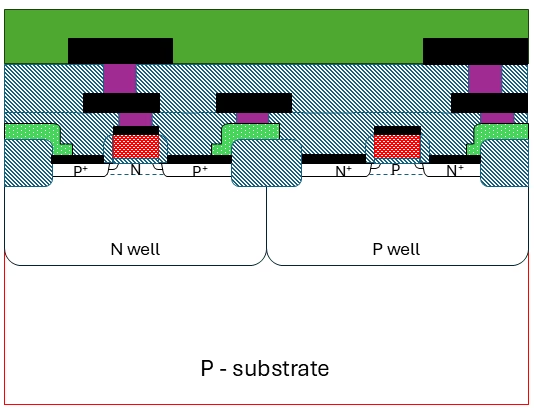
The following figure shows only the part of the transistors. Each group of transistors lays inside of a well (i.e. the orange square) that acts as a region that isolates the transistors from the substrate. Without it, parasitic effects, such as leakage current or unintented transistor actions, could occur due to the direct contact with the substrate. In the case of the top row pMOS transistors, they are placed inside an n-well, isolating them from the n-type regions. The middle row is the differential input pair, and the bottom 8 transistors are the current mirror

When zooming out, we can observe the size of the complete layout, as it also includes 7 bond pads and 10 smaller capacitances, connecte in parallel with each other. Cadence has a size limit of 900 µm2, hence I created 10 smaller ones, each 500 fF, which adds up to 5 pF. This gives a total size of the OTA of around 500 µm x 500 µm, including bond pads and the capacitance. The power consumption is around 717 µW, while we obtained a gain of 36 dB up to 1 MHz, and a GBW of 66 MHz. which means we obtained the requried specifications.
By no means is this the best layout, and a lot can be improved upon, such as the layout of the capacitors, but I hope this article helped you in some way.

Florius
Hi, welcome to my website. I am writing about my previous studies, work & research related topics and other interests. I hope you enjoy reading it and that you learned something new.
More Posts