Pin diagram
The important pins
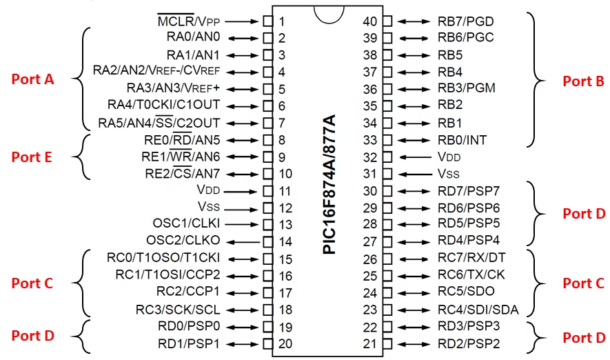
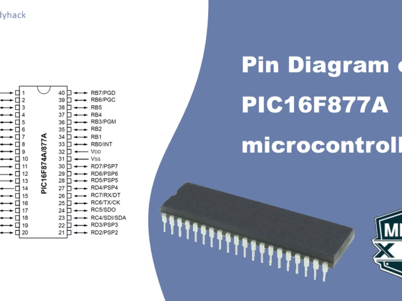
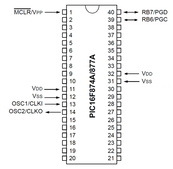
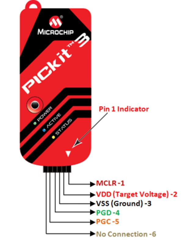
For accurate and dependable information, referring to the datasheets provided by Microchip Technology is advisable; these documents can be accessed here. Additionally, a brief overview of the pin diagram is recommended, detailing their functionalities and locations. Let’s begin by outlining the pins essential either for MCU operation or Pickit3 programmer-based programming:
- Pin 1 houses the MLCR/VPP, serving as a microchip reset mechanism.
- Pins 11 and 32, designated as VDD, necessitate a voltage range of 3.3V to 5V for proper functioning.
- Pins 12 and 31, denoted as VSS, are connecting to the ground
- To establish a connection with the Pickit3 programmer, pins 40 and 39 host PGD and PGC, respectively.
- Pins 13 and 14, namely OSC1 and OSC2, deliver a stable clock signal to the microcontroller. When utilizing the Pickit3 programmer, connecting these pins is unnecessary, thanks to the internal oscillator within the programmer facilitating MCU programming.
The exact method to program with your PICKIT3 programming tool, can be found here.
Port structure in the PIC16F877A
The PIC16F877A has 5 ports, namely A to E, where each pin can be configured as an input or output. However, it is important to note that not all ports consist of the same number of bits, due to some pins being taken by VSS or VDD, for example. In detail, port A consists of 6 bits, ports B, C, and D have 8 bits, while port E consists of only 3 bits.
Apart from being used for General Purpose Input Output (GPIO), most pins on this MCU have dedicated roles for specific functions. For instance, some pins on port C function as the TX and RX pins for the UART communication module, enabling the transmission and reception of serial data. Additionally, analog input channels for the ADC module on ports A and E can convert analog signals into digital values, opening up opportunities for further processing. When choosing IO pins, check the requirements of your project adequately to make the best possible decisions.
