The ADC module in microcontrollers indeed allows them to interface with the analog world by converting continuous analog signals into discrete digital values. This capability is crucial for various applications such as sensing, control systems, and communication. It is distinct from PWM (Pulse Width Modulation), which uses discrete pulses to simulate an analog voltage rather than directly converting it.
For this example we have an ADC that can convert an analog input signal to a 10-bit binary digital representation of that signal. The MCU’s analog inputs, which are multiplexed into a single sample and hold circuit. The output of the sample and hold is connected to the input of the ADC. The ADC generates the 10-bit binary result via successive approximation and stores the conversion result into the ADC result registers, which we will read. All of this will be explained down in the text.
1. Analog to Digital Conversion
ADC involves two key elements: the sampling frequency and the bit depth. The former determines how frequently the analog signal is sampled each second, while the latter refers to the level of detail that is obtained within each sample. Both of these aspects are critical in ensuring the accuracy and quality of the conversion process. It’s important to understand the implications of sample rate and bit depth when converting analog signals to digital format, as they have a significant impact on signal fidelity and overall performance.
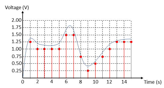
Sampling frequency
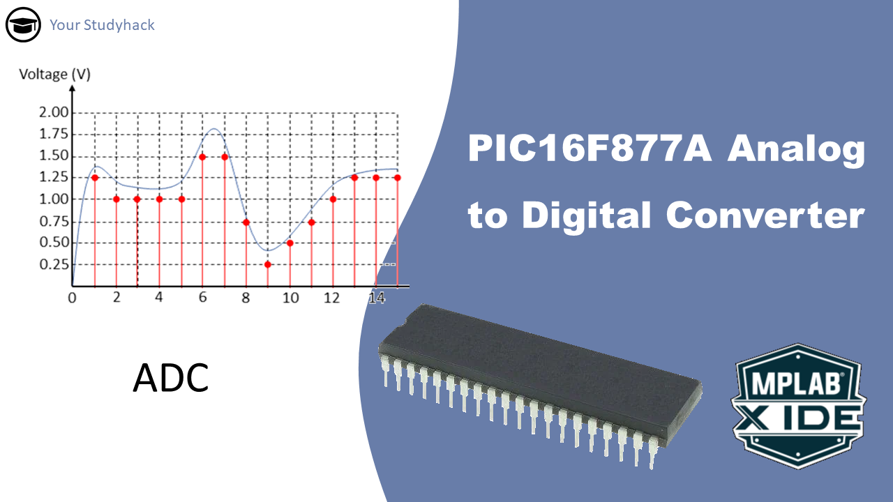
I will not go into much detail on the physics behind the sampling rate, but it has been shown that the frequency at which you sample needs to be at least twice the frequency of what is being converted. The reason for this is that if there isn’t enough sampling, some of the faster oscillations might get lost, as can be seen in Figure 1 on the x-axis.
The highest frequency that we can hear is about 20 kHz, so if this is your goal, your sampling frequency needs to be at least 40 kHz. That is the reason why the sampling rate on CDs is at 44.1 kHz.
Bit depth
Bit depth (or resolution) refers to the number of bits used to represent each individual sample in the digital representation of an analog signal. For example, if you have a 10-bit ADC, the bit depth is 10 bits, meaning each sample will be represented as a 10-bit binary value. This value determines the resolution and precision of the digital representation of the analog signal.
If we look at Figure 1, it shows an illustration of a signal being sampled with a 3-bit ADC. With 3 bits, we have 8 different levels on the y-axis. As you may see, it does not describe the signal too well, as the actual signal is quite far away from the values we can measure at, almost all the time. Increasing the bit depth will increase the resolution and better describe the actual signal.
2. ADC Initialization with PIC16F877A
The ADC module of the PIC16F877A has eight inputs, (AN0 to AN7) spread on PORTA and PORTE, and a high- and low-voltage reference input at RA2 and RA3. The conversion of an analog input signal results in an 10-bit digital number.
To initialize the ADC in this microcontroller, we first have to look at all the registers that are required to set it up. We will go over them one by one:
| Registers | Description |
| ADCON0 | This register controls the operations of the A/D module, such as channel select, on/off, etc. |
| ADCON1 | This register configures the functions of the port pins to analog inputs (RA3 can also be the voltage reference) or as digital I/O. |
| ADRESL | This register contains part of the 10-bit result of the AD conversion. |
| ADRESH | This register contains part of the 10-bit result of the AD conversion. |

ADCS2-ADCS0:A/D Conversion Clock Select bits

CHS2-CHS0:Analog Channel Select bits
000 = Channel 0 (AN0)
001 = Channel 1 (AN1)
010 = Channel 2 (AN2)
011 = Channel 3 (AN3)
100 = Channel 4 (AN4)
101 = Channel 5 (AN5)
110 = Channel 6 (AN6)
111 = Channel 7 (AN7)
GO/DONE: A/D Conversion Status bit
When ADON = 1:
1 = A/D conversion in progress (setting this bit starts the A/D conversion which is automatically cleared by hardware when the A/D conversion is complete)
0 = A/D conversion not in progress
ADON: A/D On bit
1 = A/D converter module is powered up
0 = A/D converter module is shut-off and consumes no operating current
To initalize, we just have to set the frequency with ADCS2-ADCS0 bits, and turn on the ADC module with ADON = 1;

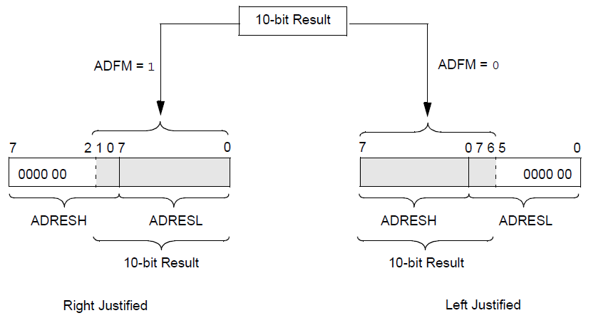
ADFM: A/D Result Format Select bit
1 = Right justified. Six (6) Most Significant bits of ADRESH are read as ‘0’.
0 = Left justified. Six (6) Least Significant bits of ADRESL are read as ‘0’.
ADCS2: A/D Conversion Clock Select bit
Check ADCS1:ADCS0 of ADCON0 register.
PCFG3-PCFG0: A/D Port Configuration Control bits
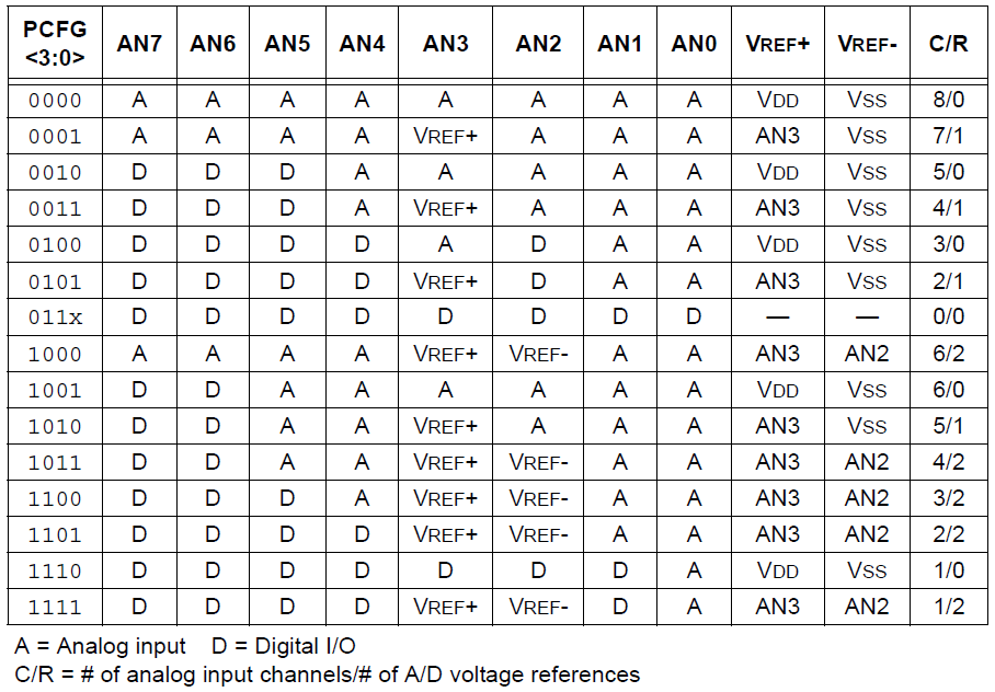
In this tutorial we will use a frequency FOSC/16. Hence the ADCS2-ADCS0 bits are set to 101. Do note that ADCS2 is located in ADCON1 register and ADCS1-ADCS0 is located in the ADCON0 register. Furthermore, we will right align our result format by setting ADFM = 1;
Due to the fact that we will obtain a 10-bit result, it has to be split over two 8-bit registers, namely ADRESH and ADRESL. We can align it to the right or to the left as shown in Figure 2. The justification for right or left is up to your own preference, but I prefer to work with Right Justified mode.
For the initialization we then obtain:
- ADCON0 = 0b01000001;
- ADCON1 = 0b11000000;
3. Reading an ADC Value
3.1 Selecting AN channel
After initialization, we need to select which analog input(s) we want to use. In certain PIC controllers, TRISx is used to set it as IO, while an ANSEL register sets it as analog (or digital if not set). However, in the PIC16F877A this is done differently. If we look at the ADCON1 register, we see that for PCFG3-PCFG0 we can have different options. We have 15 different options to set certain ports to analog or digital. For this tutorial I will use only a single analog input, namely AN0. Hence we set PCFG3-PCFG0 = 1110;
If you’d require a different start- or end-voltage, you can use one of the other options and set VREF+ and VREF– to the right voltages. In that case we set PCFG3-PCFG0 = 1111;
It is also possible to have multiple analog inputs connected to your microcontroller. For this, we have many options, and it depends on your project. However, if you do want to obtain multiple analog inputs and convert them to digital, know that there is only a single ADC module. You will have to alter the code that will make it rotate between the different analog inputs. This is done in the next part.
We’ll also have to look at the ADCON0 register. Here we can select which channel we want to read from by setting the CHS2-CHS0 bits. As I’ve mentioned before, we will use AN0, hence we set CHS2-CHS0 = 000; When you have multiple analog inputs, you will have to rotate them using your program.
3.2 Starting Conversion
Once the correct channel is selected, we start the conversion by setting the ADCON0bits.GO= 1; The conversion is in progress and it will be automatically cleared by the hardware when it is done. Best is to make a simple while loop, which stops once it is cleared.
while(ADCON0bits.GO); // Wait for A/D Conversion to complete
3.3 Reading ADC results
At the moment, the 10-bit result will be ready, but split into two different registers (ADRESH and ADRESL). ADRESH only contains the 2 MSBs, while ADRESL has all 8 LSBs.
For me, justifying the results to the right felt like the easiest option. Because if you want to create a 16-bit value by directly concatenating the bits from ADRESH and ADRESL, you can use a simple bitwise shift and OR operation as follows:
					    result = ((uint16_t)(ADRESH) << 8) | (uint16_t)(ADRESL); // Creating 16 bit int with 10-bit result
    return result;
This code will left-shift the 8 bits from ADRESH by 8 positions to make them the 8 most significant bits (MSBs) of the 16-bit result. Then, it directly combines them with the 8 bits from ADRESL using a bitwise OR (|) operation to form a 16-bit value.
Given your example values (all ones):
ADRESHis0b00000011ADRESLis0b11111111
This code will return 0b0000001111111111
Lorem ipsum dolor sit amet, consectetur adipiscing elit. Ut elit tellus, luctus nec ullamcorper mattis, pulvinar dapibus leo.
4. Programming Code for MPLAB
In this example, we have a sensor on AN0, which requires a full range of 0V to 5V. We want to convert this analog signal into a digital one.
To display the value using an LCD or 7-segment display, I refer you to those pages.
					#include <pic16f877a.h>
#include <xc.h>

// Define the frequency of the external crystal oscillator
#define XTAL_FREQ 20000000  // 20MHz external crystal oscillator frequency

// Configuration bits
#pragma config FOSC = HS    // High-Speed Crystal oscillator
#pragma config WDTE = OFF   // Watchdog Timer disabled
#pragma config PWRTE = OFF  // Power-up Timer disabled
#pragma config BOREN = OFF  // Brown-out Reset disabled
#pragma config LVP = OFF    // Low-Voltage Programming disabled
#pragma config CPD = OFF    // Data memory code protection off
#pragma config WRT = OFF    // Flash Program Memory Write protection off
#pragma config CP = OFF     // Flash Program Memory Code protection off

// Initialize ADC
void ADC_Initialize() {
    TRISAbits.TRISA0 = 1; // RA0 is set to input. RA0 = AN0
    ADCON0 = 0b01000001;  // Fosc/16 is selected and ADC is ON.
    ADCON1 = 0b11000000;  // Right Justified and only AN0 is an analog input, with VDD and VSS as +/- reference.
}

// Read ADC. Further changes can be made if you want to change the channel
unsigned int ADC_Read() {
    unsigned int result;
    __delay_us(10);       // Acquisition Time - increase it if something goes wrong
    ADCON0bits.GO = 1;    // Starts A/D Conversion
    while(ADCON0bits.GO); // Wait for A/D Conversion to complete
    result = ((uint16_t)(ADRESH) << 8) | (uint16_t)(ADRESL); // Creating 16 bit int with 10-bit result
    return result;
}

void main(){
    unsigned int adc;

    ADC_Initialize();

    while(1){
    adc = ADC_Read();
    __delay_ms(1000); // Just putting a delay of 1 second here,
                      //you might want to display it on LCD, or 7segment display, etc.
    }
}
4.1 additional code
When using multiple analog inputs, your ADC_Read() function requires the variable “channel”. In addition to the code, make sure you do the following as well:
- Make sure the A/D Port Configuration Control bits (PCFG3-PCFG0) are set correctly to have multiple analog inputs
- Set the analog pins you use as input using the TRISx register.
					unsigned int ADC_Read(unsigned char channel) {
    unsigned int result;
    __delay_us(10);            // Acquisition Time - increase it if something goes wrong

    // Set the ADC channel based on the 'channel' argument
    ADCON0 = (ADCON0 & 0b11000111) | (channel << 3);

    ADCON0bits.GO = 1;         // Starts A/D Conversion
    while(ADCON0bits.GO);      // Wait for A/D Conversion to complete
    result = ((uint16_t)(ADRESH) << 8) | (uint16_t)(ADRESL); // Creating 16-bit int with 10-bit result
    return result;
}
Florius
Hi, welcome to my website. I am an electronic enthusiast, writing about my previous studies, work & research related topics and other interests. I hope you enjoy reading it and that you learned something new.
More PostsYou may also like


