Most microcontrollers have a limited current sink or current source on the pins, the PIC16F877A is no exception. However, for certain projects you may want to use larger currents then just 25mA, which is the max current source for this microcontroller. For those kind of projects you’ll have to resort to using transistors. In this tutorial we will look at some of the options how to control BJTs, and discuss what is possible and how to set them up correctly in your own project.
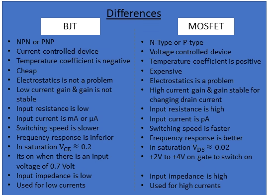
There are two main types of transistors, the Bipolar Junction Transistor (BJT) and the Metal-Oxide-Semiconductor Field-Effect Transistor (MOSFET). Both of them have been created in the late 40s and 50s of the last century. Both are important semiconductor devices with distinct characteristics and applications. Understanding the differences between the two can help you choose which one you will need for your project. For the explanation of interfacing your microcontroller with a MOSFET, please see part 2 of this series. I will list some of the most important differences here:
1. Bipolar Junction Transistor
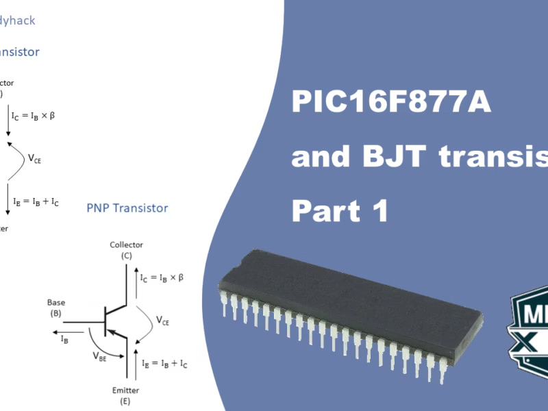
A BJT is a three-terminal semiconductor device that is widely used in electronics for amplification, switching, and signal processing. It consists of three layers of semiconductor material: the emitter, the base, and the collector. These layers are typically made of silicon. The two types of BJTs are NPN and PNP, which have slightly different layer arrangements.
The transistor functions as a current amplifier. When a current is fed into the base terminal, it gets magnified by the current gain factor of the transistor, denoted as β. As a result, the transistor can be employed as an amplifier. A very small current at the base terminal, is enlarged by a factor of β, which flows as a collector current on the collector terminal side.
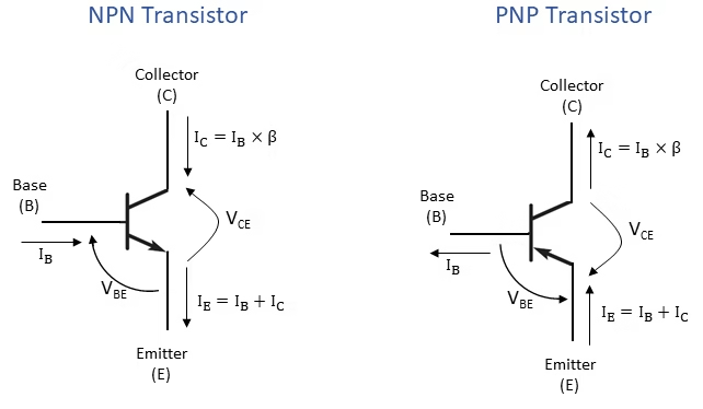
The NPN and PNP transistors both have three states of operation. This discussion will focus on the NPN transistor; however, similar calculations also apply to the PNP transistor. The three stages are as follows:
- The off state (cutoff region) occurs when the transistor is not conducting any current from its collector to emitter. In this state, the base-emitter junction is below the threshold voltage, and no current can pass through the base, resulting in no significant collector current (IC).
- The linear state, (Amplification region), is where the NPN BJT functions as an amplifier. In this state, the voltage applied to the base is sufficient to overcome the barrier. Consequently, a small current will flow (IB), creating a substantial collector current (IC = β x IB). In this regime, doubling the base current would also double the collector current; thus, it is called the linear state. This state is typically used for analog amplifiers (Class A Amplifier).
- The saturated state occurs when increasing IB further will not lead to a change in IC since the voltage drop VCE reaches the power supply. This saturation would distort amplification by clamping the output signal.
2. BJT as a switch
In Figure 2, we can see the 3 states and voltage and current conditions with those states. in the Off state, the voltage across the collector and emitter, VCE, is the same as the supply voltage; this is similar to an “open switch“. When the circuit is in the Saturated state, VCE is below 0.2V and acts as an closed circuit; hence it similar to a “closed switch“.
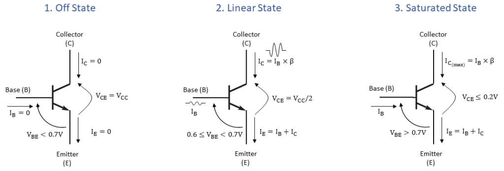
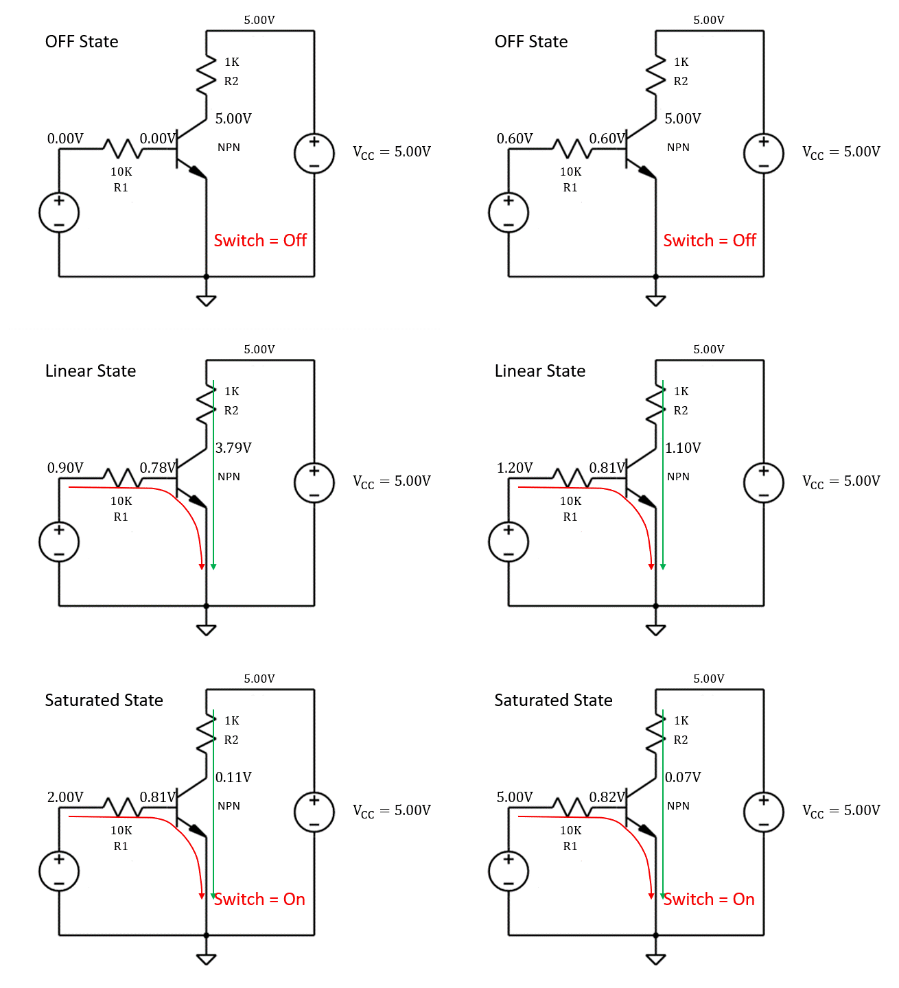
Figure 3 shows an animation of the three states for different voltages on the base, ranging from 0 to power supply (5V). In this example, we assumed no IB below 0.7V and we took β = 100. We notice that for voltages below the treshold voltage of 0.7V, it is in the Off state. Only once we reach a couple of volts, do we actually enter the saturated state. But this works fine for microcontrollers where we can apply either ground or 5V on the output pins, allowing the transistor to work as a switch.
2.2 Practical example 1 - Calculating RB & RC
One of the cheaper BJT transistors out there, is the 2N3904, with a maximum collector current (continuous) of IC = 200 mA, VCE saturate = 0.2 Volt, VBE saturate = 0.65 Volt and a gain β = 100 to 300.
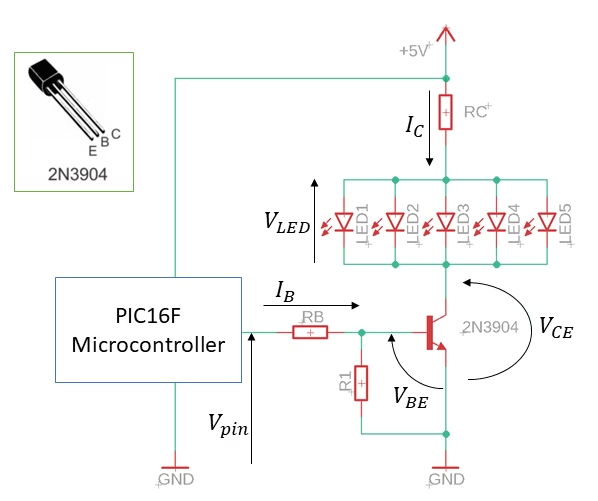
In this example, we will make some assumptions to make the calculations manageable.
- No current will flow through RB in the Off state.
- We set VBE = 0.7 V, which is a more general value.
- We set VCE = 0 V.
- The gain β = 100.
- VLED = 2V, with a consumption of 15 mA per LED.
- Vpin = 5 V
- Rule of thumb: Always stay below half the maximum IC continous current ≈ 100 mA.
1.2.1 Calculating RC
Based on the specifications of 5 LEDs that we have, the total IC current comes to 75 mA, which is well below the maximum 100 mA limit we had set earlier. We would need to look for another transistor if the current exceeds the limit. The value of resistor can be calculated using the formula:
\[RC = \frac{V_{CC}-V_{LED}}{I_C} = \frac{5-2}{0.075} = 40 \Omega\]
\[P = V_{CC}-V_{LED}\times I_C = (5-2)\times 0.075 = 0.225W\]
The nearest highest value resistor that can handle 0.225 W would be 47 Ohm, 0.250W resistor. However, for better heat dissipation, it is recommended to double the value to a 0.5 W, 47 Ohm resistor.
1.2.2 Calculating RB
We know we have a gain of 100, hence the base current is 100 times lower the value of the collector current. With a collector current of 75 mA, we can calculate IB using the formula:
\[I_B = \frac{I_C}{\beta} = \frac{75 mA}{100} = 0.75 mA\]
This shouldn’t be an issue for the microcontroller, which normally has a maximum current source of around 25 mA. From here we can calculate the resistance RB, because we know the voltage across the pin is 5V, which should be equal to the voltage drop across the resistor and VBE combined.
\[RB = \frac{V_{pin}-V_{BE}}{I_B} = \frac{5-0.7}{0.75\times 10^{-3}} = 5733.33 \Omega\]
\[P = (V_{pin}-V_{BE})\times I_B = 0.003225 W\]
The nearest highest value resistor that can handle this Wattage is a 6200 Ohm, 0.25W resistor.
1.2.3 Reality is not the same
In reality, the characteristics of the transistor might not be exactly what we assumed; e.g. the gain is not 100, and can change from transistor to transistor, current flowing through it, ambient temperature and more. In the datasheet you can find more information on how the gain changes.
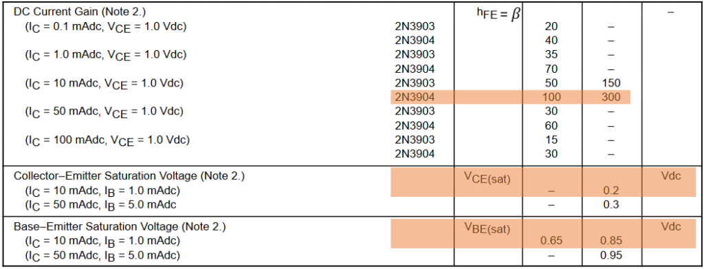
In the previous method used to calculate RB, there was an element of chance involved, as it relied on having enough gain to be in the saturation regime. In that calculation the value of RB can be considered a higher limit case. A more reliable approach is by disregarding the gain factor and setting the base current at 1/10th of the collector current, without considering the gain at all. Redoing the calculation will give you the following:
\[I_B = \frac{I_C}{10} =\frac{75}{10}= 7.5mA\]
\[RB = \frac{V_{pin}-V_{BE}}{I_B} = \frac{5-0.7}{7.5\times 10^{-3}} = 573.33 \Omega\]
For most practical applications, we can double this value and look for its nearest highest value resistor: 1.2 kOhm. Of course, making a test setup, and measure the voltages, etc. will give you a better estimate, as each transistor is different. Obtaining the actual characteristics of your device will be even more helpful for fast-switching transistors, as pushing it all the way into saturation will increase its switching time.
1.2.4 Calculating R1 - Thevenin equivalent circuit
We have not yet discussed the function of pull-down resistor R1. This resistor is placed here to make sure the transistor is off when small leakage current is present, and is normally much larger than RB. In this case we can set it to 10 kOhm. This does change the original voltage we used for Vpin. A reiteration can be made to get a more exact value. It will not change the results too much, but I will explain here how it is done.
We can replace the original circuit, depicted in Figure 6 on the left, with the Thevenin equivalent circuit on the right. using the following formulas, we can calculate that Vth = 4.46 Volts and Rth = 1071 Ohm.
\[V_{th} = V_{pin}\times\frac{R1}{R1+RB}\]
\[R_{th} = R1\parallel RB = \frac{R1\times RB}{R1 + RB}

3. BJT as a class A amplifier
A Class A amplifier is a type of electronic amplifier that operates in such a way that its output transistors are always conducting current, even when there is no input signal. It’s designed to provide a high-quality output with low distortion and is often used in applications where audio fidelity is crucial, such as in high-end audio systems and professional audio equipment. One of the drawbacks of Class A amplifiers is their relatively low efficiency. Since the output transistors are always conducting, they consume power even when no input signal is present. This results in significant power wastage as heat, making Class A amplifiers less energy-efficient.
To make the transistor work as an amplifier, you want to configure the transistor in the linear regime. Once you can have it in the ON state (either linear or saturated), any change in voltage on the input will give a change on the output. When the input voltage is high, the current is high, hence the voltage drop is high and the output is low. Similarly, when the input turns low, the output turns high. The output has a phase shift of 180 degrees. On top of that, the signal looks distorted, as the gain of the transistor is too high and it is getting saturated. This is best shown in left side of Figure 7.
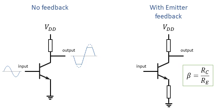
To limit the gain (and saturating the signal), we need to provide feedback as shown in Figure 7, on the right side. Hence we add a resistor between the emitter and the ground. This configuration is commonly known as “emitter degeneration”. When a resistor is placed on the emitter side of the transistor, it creates a voltage drop across the resistor as the emitter current flows through it. This voltage drop subtracts from the voltage at the emitter terminal, effectively reducing the voltage available to the base-emitter junction. The emitter resistor reduces the amount of base current that flows into the transistor. This, in turn, affects the collector current and the overall gain of the transistor. By controlling the amount of emitter current, the resistor stabilizes the transistor’s bias point, making it less sensitive to variations in transistor parameters, temperature, and external factors. Due to the feedback, the gain will be:
\[\beta = \frac{R_C}{R_E}\]
Next we add a capacitor at the output to remove the DC bias and just get the amplified input signal. We know that transistors need approximately 0.7V at the base to turn on; that means small signals below this threshold cannot be amplified. To make this work, we need to add a DC bias to the input signal, such that the small input signal is always above the threshold voltage. To do that, an additional voltage divider is placed. To allow only small ac signals to pass, we also add a capacitor at the beginning. It is common to add a capacitor in parallel to the emitter resistor as well. Figure 8 shows how it looks.
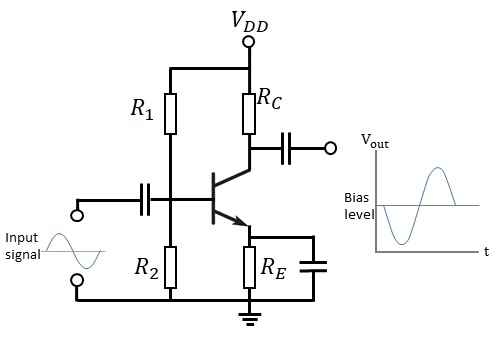
The values of the resistance depend on the type of signal you want to amplify. Best is to use programs such as LTSpice to test out your particular case. For my own project I used the values:
- RE = 3.3 kOhm
- RC = 12 kOhm
- R1 = 10 kOhm
- R2 = 1.2 kOhm
- Transistor BC550
- VDD = 15 V
- Small ac-signal 50 mV
- All capacitors depend on the lowest frequency you want to let through: 1 / (2πfC)
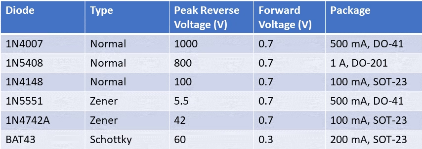
4. Common Types of Diodes and Transistors
Here I provide you with a comprehensive overview of some of the most commonly used BJTs and diodes suitable for hobbyists.

5. Summary
This tutorial provides an overview of the three states of bipolar junction transistors. While the Off- and Saturation-states serve as effective switches, the Linear state is often utilized in various types of amplifiers. It is worth noting that transistors require in-series resistance on the Base and a pull-down resistor to function correctly. As demonstrated, we have examined how to determine their values both in theory and practical settings. Additionally, we only briefly touched upon class A amplifiers as they represent a distinct field of analog devices outside of the scope of this tutorial.
Florius
Hi, welcome to my website. I am writing about my previous studies, work & research related topics and other interests. I hope you enjoy reading it and that you learned something new.
More Posts

