



Most microcontrollers have a limited current sink or current source on the pins, the PIC16F877A is no exception. However, for certain projects you may want to use larger currents then just 25mA, which is the max current source for this microcontroller. For those kind of projects you’ll have to resort to using transistors. In this tutorial we will look at some of the options, and discuss what is possible and how to set them up correctly in your own project.
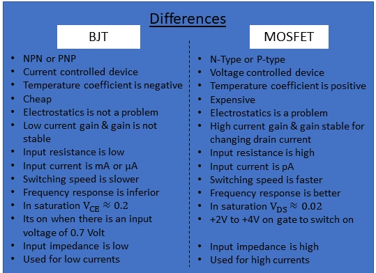
There are two main types of transistors, the Bipolar Junction Transistor (BJT) and the Metal-Oxide-Semiconductor Field-Effect Transistor (MOSFET). Both of them have been created in the late 40s and 50s of the last century. Both are important semiconductor devices with distinct characteristics and applications. Understanding the differences between the two can help you choose which one you will need for your project. For the explanation of interfacing your microcontroller with a BJT, please see part 1 of this series. I will list some of the most important differences here:
1. MOSFET
A MOSFET, or Metal Oxide Semiconductor Field Effect Transistor, distinguishes itself from a Bipolar Junction Transistor (BJT) by being a Unipolar Device. This implies that it exclusively employs the majority carriers for conduction. However, in the construction of power MOSFETs at the silicon level, an unintended parasitic anti-parallel diode is incorporated across the drain and source. This peculiarity causes the MOSFET to conduct when the voltage across it is reversed, a factor that warrants consideration. The majority of power MOSFET schematic symbols portray this parasitic diode as part of the depiction.
The operational principle involves utilizing an insulated gate separated from the channel. The crucial factor that governs its conductivity is the voltage applied at the gate terminal.
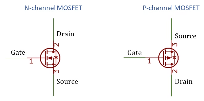
As for its terminals, a standard MOSFET is designed as a 3-terminal device: Gate (G), Source (S), and Drain (D). Notably, there exists a fourth terminal known as the Substrate or Body terminal; however, it is typically omitted from either input or output connections and not extensively used in regular applications. The schematics of an N-channel and P-channel MOSFET are shown in Figure 1.
The N-Channel and P-Channel MOSFETs have 3 regimes in which they can work. This discussion will focus mainly on the N-Channel MOSFET, however, similar calculations also apply to the P-Channel MOSFET. The three stages are as follows:
- Cut-Off Region: In the cut-off region, the MOSFET is effectively turned off. Both the gate-to-source voltage (VGS) and the drain-to-source voltage (VDS) are insufficient to create a conducting channel between the source and drain. As a result, the MOSFET exhibits very high resistance, effectively blocking the flow of current from drain to source.
- Linear (or Triode) Region: In the linear region, the MOSFET operates as an amplifier. By applying a sufficient gate-to-source voltage, an inversion layer is formed under the gate oxide, creating a conducting channel between the source and drain. The width of this channel is modulated by the gate voltage. As the drain-to-source voltage increases, the channel starts to narrow due to the voltage drop across it, leading to a region where the MOSFET acts like a variable resistor, hence it is called linear region.
- Saturation Region: In the saturation region, the MOSFET operates as a closed switch. The gate-to-source voltage has already created a conducting channel, and the channel is “pinched off” by the drain-to-source voltage. This pinching off prevents the channel from narrowing further, resulting in a relatively constant channel width, and the current won’t increase further. The MOSFET acts as a low-resistance path between the source and drain, allowing a significant current to flow even for small changes in VDS.
1.1 MOSFET characteristic curve
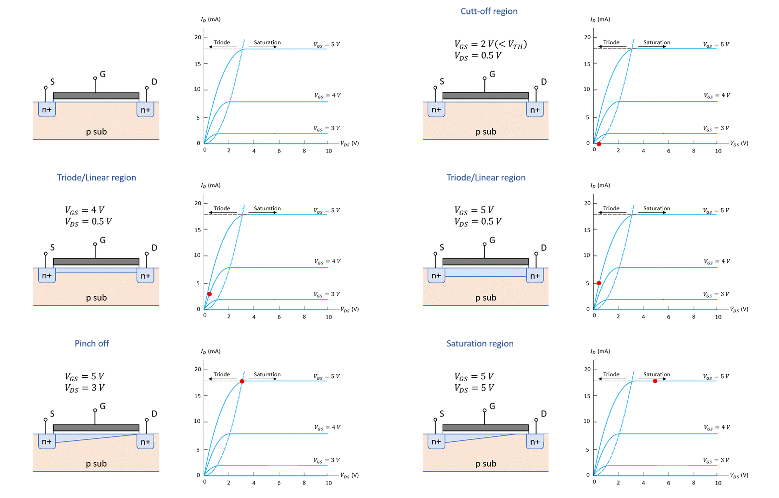
This animation shows the structure of the MOSFET on the left side and the corresponding current as a function of VDS, for different values of VG on the right side. I will briefly give some comments on what is happening for the different values that we applied on VGS and VDS in this example.
- We know that VGS needs to overcome a threshold to create a conducting channel between S and D; in this example, only when VGS ≥ 3 Volts, it overcomes the threshold. Increasing VGS further, will increase the the width of the channel more.
- Applying a small VDS allows the current to flow from drain to source. As you increase VDS further, the channel becomes narrower at the D side, until it “pinches off”. This narrowing of the channel does not mean that the current is blocked off, it refers to limiting the increase in current. From this point onward, the current is constant (in practice it is not entirely as I explain shortly).
- Increasing VDS further will get you in the saturation region. There is now a gab in the channel at the drain side. Due to the large potential, the electrons will still pass and actually get accelerated across it. Hence in practice the ID current will still slightly increase when an increasing VDS. This is however, not shown here.
2. MOSFET as a switch - Practical example
In a scenario where a 12W load (+12V, 1A) needs to be managed with a microcontroller, a bridging device must be implemented, as the microcontroller itself cannot provide the required power. It is imperative that this bridging device can be controlled by the microcontroller, while simultaneously supplying sufficient power to the load. To address this, a MOSFET can be utilized as the bridge component, as illustrated in Figure 2.

As MOSFETs are voltage controlled devices, all we need to do to turn it on, is to set the output of the microcontroller to a logic “1” (assuming a 5V microcontroller, such as the PIC16F877A). Similarly, we can turn off the MOSFET by setting the output to a logic “0”. Thus, controlling the load can be done digitally.
2.1 Power dissipation
This doesn’t sound difficult, but you’ll have to choose the right MOSFET for the job. Let’s take another look at the example: Let’s assume the resistance in channel (RDS) is about 0.1 Ohm. The power dissipated in this device is calculated by the formula:
\[P = I^2\times R = 1^2\times 0.1 = 0.1 W\]
This doesn’t seem like a lot, but when you are driving a motor from stand still, it has to overcome the initial inertia. This initial surge in current can be quite large and it might cause the MOSFET to overheat and break down. A solution to this could be to mount a heatsink to the MOSFET package. Another solution is to use power MOSFETs, as they have a surge-current protection built into their design.
2.2. Logic Level MOSFETs
It is also important to consider the logic level required to control a MOSFET. For instance, the maximum output level of certain microcontrollers, such as PIC16F877A, may not be adequate to fully saturate the MOSFET. In such cases, low-threshold MOSFETs, which are compatible with TTL and CMOS logic gates as low as 1.5V to 2V, could be used instead.
2.3 Explanation of the circuitry
As you might have noticed, we have not fully explored the schematic yet. This is partly, because there is not much to calculate for this type of configuration. However, we will go over the components to explain why we use them.
- Pull-down resistor. Similar to a standard capacitor, the gate of a MOSFET retains its stored charge unless it is intentionally discharged or naturally dissipates through minimal gate leakage current. A scenario could arise when the driving circuitry leaves the gate disconnected, or “floating.” If stray charges accumulate in the gate to an extent where they exceed the threshold, the MOSFET can unintentionally turn on, which could damage the circuitry. It is a common practice to use a pull-down or pull-up resistor between the gate and source terminals. This resistor serves the purpose of discharging the gate when the gate voltage is removed. A value of 10K ohms is often deemed suitable.
- Small series resistor: The gate capacitance (the inherent capacitance between the gate and source terminal) and the inductance of the connecting leads can interact to create transient voltage spikes or oscillations. To mitigate these oscillations, a resistor of 10 Ohms is added to in series with the gate to help dampen the rapid voltage changes and dissipate some of the energy.
- Zener diode: The gate terminal is very sensitive because of the extremely thin layer of oxide underneath. The use of a Zener diode across the gate is a protective measure to limit the voltage at the gate and prevent it from exceeding the MOSFET’s specified maximum gate-source voltage. The Zener diode’s breakdown voltage acts as a threshold, ensuring that any voltage spikes due to ESD or other transients are clamped at a safe level before they reach the MOSFET’s gate. Remember that MOSFETS are very sensitive to electrostatic discharges, so handle them with care!
- Flywheel diode:
When dealing with inductive loads (e.g. electric motors, transformers, relays, and inductors), a flywheel diode is placed across the load to effectively mitigate the impact of any back electromotive force (EMF) generated during the load’s deactivation. The rationale behind this practice lies in the inherent behavior of inductive loads: when a current courses through the coil of a device such as an electric motor, it engenders a magnetic field that stores energy. However, when the flow of current is abruptly halted—such as during the deactivation of the motor—this stored energy seeks a path for release, giving rise to a voltage spike in the opposing direction.
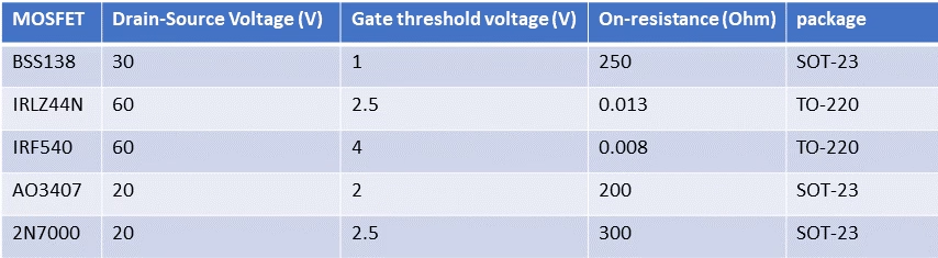
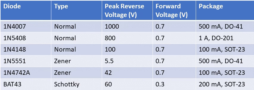
3. Common types of MOSFETs and diodes.
Here I provide you with a comprehensive overview of some of the most commonly used MOSFETs and diodes suitable for hobbyists.
4. Summary

Florius
Hi, welcome to my website. I am writing about my previous studies, work & research related topics and other interests. I hope you enjoy reading it and that you learned something new.
More PostsYou may also like