
In the early days of integrated circuits, NMOS was the preferred choice due to its speed and compact design compared to earlier technologies like PMOS. However, NMOS had a major drawback—it continuously consumed power. Unlike CMOS, which only draws power during transitions, NMOS logic relied on a resistive pull-up network, causing a constant current flow even when the transistor was not switching. This led to high power consumption and excessive heat, making NMOS increasingly difficult to scale.
Table of Contents
CMOS cicuits solved this issue by using a complementary pair of transistors (NMOS and PMOS). At any given time, one transistor is always off, effectively blocking current flow. As a result, CMOS consumes virtually no static power, except for a small leakage current. This efficiency allowed for higher transistor densities without overheating, enabling the continued scaling of integrated circuits and driving the steady progress of Moore’s Law.
CMOS Integrated Technology
Figure 1 illustrates the cross-section of a CMOS integrated circuit, with a PMOS transistor on the left and an NMOS transistor on the right. You might wonder why an NMOS device isn’t built directly in the P-substrate without adding a P-well. In practice, the twin-well process—which includes both N-well and P-well—is far more common. This is because the doping process for creating a P-well is more controlled than doping the entire substrate. Additionally, since N-wells and P-wells have similar doping levels, it is easier to start with a lightly doped substrate and then tailor each well specifically for its respective device.

Note that in all the figures, layer thicknesses are not to scale. For reference, Si₃N₄ is typically around 100 nm thick, while the photoresist layer is about 10 times thicker. The substrate, in turn, is roughly 500 times thicker than the photoresist layer. Additionally, mask fabrication is extremely costly, often ranging from a few million dollars per mask due to the need for extreme precision. As a result, if a process step can be designed to eliminate the need for a mask, it is typically done to reduce costs.
In the following sections, I will explain the process steps of the early CMOS technology from the early 1980s in semiconductor manufacturing. In particular the range from 3 μm down to 1 μm. This refers to the minimum size of the gate length of the transistor. 3 µm technology is still used for certain types of chips, but it is typically reserved for less complex, lower-performance applications where the latest and smallest nodes (e.g., 5 nm or 7 nm) are not necessary, such as RF chips, or in safety-critical systems like microcontrollers and signal processing.
Substrate Selection
Before creating semiconductor devices, it is important to select the appropriate wafer. Key design parameters include crystal orientation, doping type (N or P), resistivity, and wafer size. Since most NMOS technology was originally developed on P-type substrate wafers, it became standard practice to continue using the same processes, making them more cost-effective and widely available.
For P-substrate wafers, the doping concentration is typically on the order of 1015 cm-3. As will become more apparent later, the doping levels in the wells are typically in the range of 1016 – 1017 cm-3.
Another critical parameter is crystal orientation. Today, almost all microchips are fabricated on wafers with a (100) surface orientation. This is primarily due to the Si/SiO2 interface quality—the (100) orientation has fewer defects and a lower interface state density compared to other orientations, making it ideal for MOSFET fabrication.
Isolation - Active Area definition
Modern CMOS chips are fabricated side by side on a silicon wafer, so it is necessary to define the area of each individual chip. The first step in this process is to clean the wafer to remove any surface impurities.
Next, a SiO2 layer is grown by placing the wafer in a furnace at 900°C for approximately 15 minutes. This results in an oxide layer that is 40 to 60 nm thick.
Following this, a silicon nitride (Si3N4) layer is deposited in a second furnace using a chemical reaction. This layer, typically 80 to 120 nm thick, plays a crucial role in the LOCOS (Local Oxidation of Silicon) process by preventing oxygen from reaching certain areas of the silicon substrate. This helps in defining the active regions of the chip. Finally, as shown in Figure 2, a photoresist layer (1 μm) is applied to the wafer using a photoresist spinner. This process requires a certain expertise to ensure that the photoresist is uniformly distributed across the wafer.
After these steps, the wafer is baked at 100 °C, and a first mask is used to expose the photoresist, defining the pattern for the LOCOS regions. In this process, a positive photoresist is used. The light-sensitive molecules in the resist absorb UV photons, causing a chemical change in their structure. When placed in a developer solution, the exposed areas dissolve, leaving the silicon nitride exposed in certain regions. An etching system, such as the MRC Reactive Ion Etcher (RIE), is then used to etch the silicon nitride layer down to the silicon oxide, as shown in the bottom part of Figure 2. Once the Silicon Nitride has been etched, the photoresist can be chemically removed in sulfuric acid, which does not significantly interact with the other layers.

Local Oxidation of Silicon (LOCOS)
After the photoresist is removed, we are left with defined areas of silicon nitride on top of the silicon oxide layer. The wafer is then placed into a furnace in an oxidizing environment, where a thick layer of SiO₂ grows. The silicon nitride acts as a barrier, preventing water and oxygen from diffusing into the substrate, which would otherwise cause oxidation. As a result, SiO₂ grows only in specific regions where it is exposed to the air, reaching a thickness of approximately 500 nm. During this process, some of the reactions also happened slightly under the silicon nitride, where it gets pushed upwards. This is illustrated in figure 3. After the furnace operation, the Silicon Nitride layer can be removed, there are different methods, but one could be phosphoric acid, which is highly selective between the Silicon Nitride layer and Silicon oxide. We are now left with thick isolation barriers that can be used as isolations between different MOS devices.
I previously introduced this technique in the NMOS fabrication process. The LOCOS (Local Oxidation of Silicon) technique has both advantages and disadvantages. On one hand, it defines the active regions for devices, but on the other, as devices shrink, the loss of surface area increases, reducing device density. In a future article, I will explain the solution to this problem: the Shallow Trench Isolation (STI) technique.

Well Formation
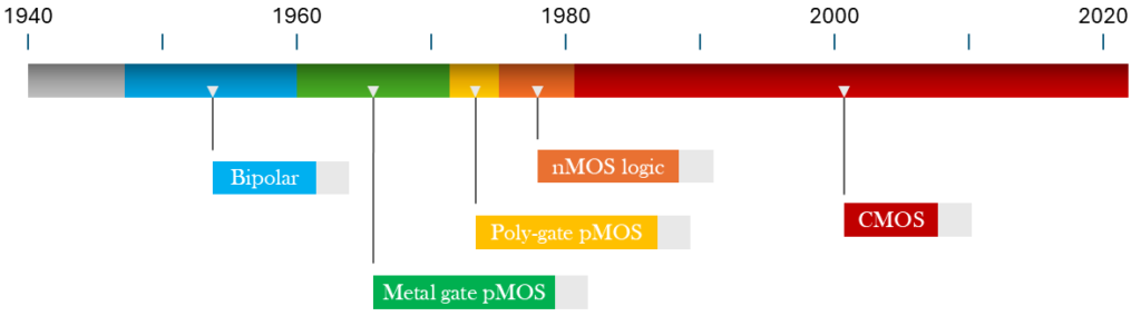
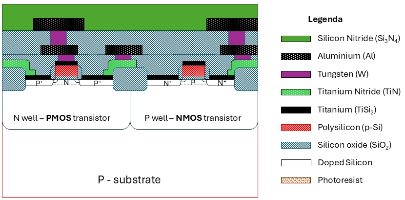
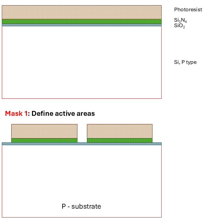
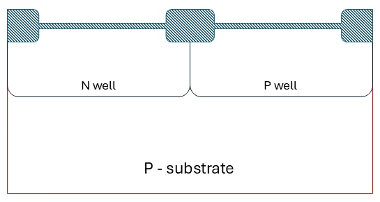
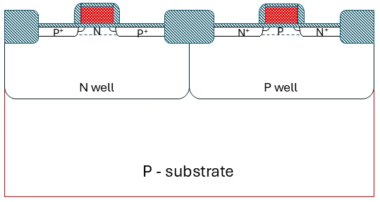
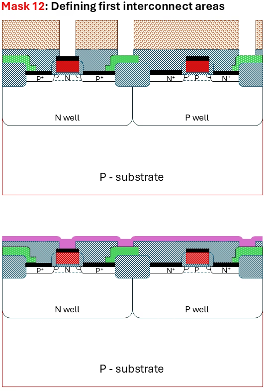
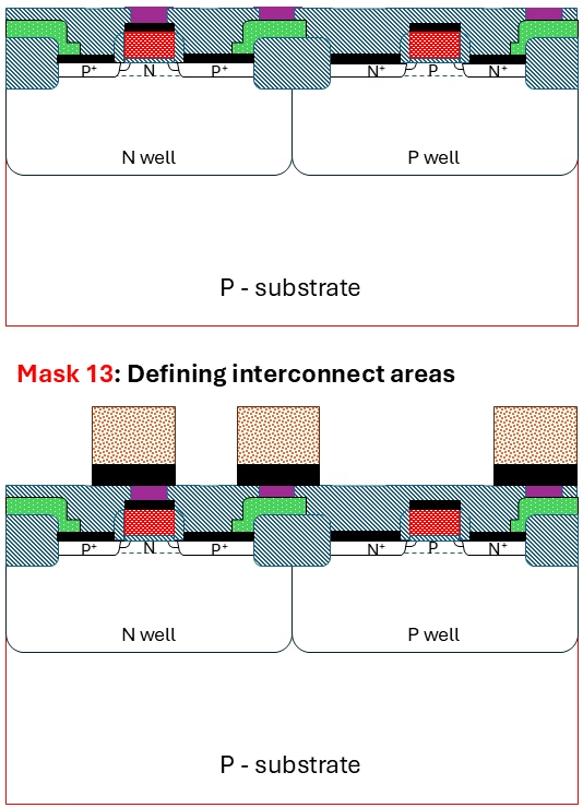
With the previous step, we created isolation barriers and therefore defined the areas where the active devices are placed. The next step is to create N-type and P-type wells. These wells have specific local doping that provide optimal device characteristics such as threshold voltage, I-V characteristics, PN junction capacitance, and more.
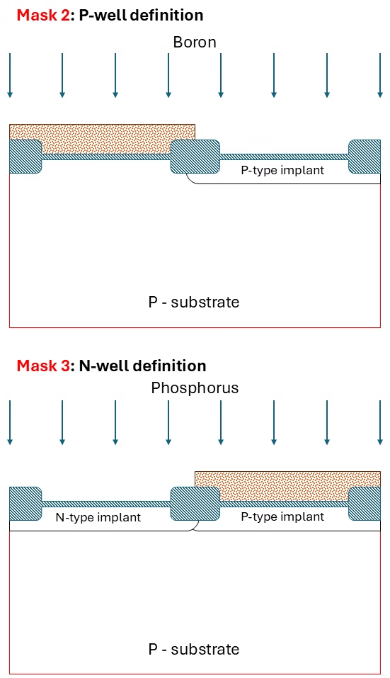
We start with spin-coating photoresist on the wafer and use a second mask to define the regions for the P-wells. We implant Boron (B⁺) ions onto the wafer through a process called Ion Implantation (II). This is done with sufficient energy to penetrate the silicon oxide but not the photoresist.
Importance of Proper Doping:
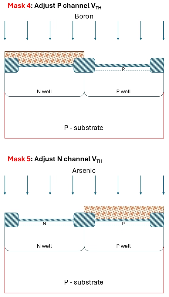
The proper doping profile is crucial to prevent unwanted conduction paths. If the threshold voltage of the isolation regions is too low, surface inversion can occur, allowing unintended electrical connections between neighboring MOS transistors.
Ion Implantation Considerations:
The ion energy must be carefully calibrated, as implantation disrupts the silicon crystal structure. For optimal MOS transistor performance, a high-quality crystalline substrate is required. To repair implantation-induced damage, the wafer undergoes a high-temperature annealing process in a furnace.
After the Boron implant is complete, the photoresist is removed using either chemical stripping or O₂ plasma etching. A new layer of photoresist is then applied, and a third mask is used to define the N-well regions. The process is identical to the P-well formation, except that the dopant is phosphorus. While several N-type dopants exist (phosphorus, arsenic, antimony), phosphorus is commonly used due to its similar diffusion coefficient to boron, resulting in comparable junction depths.

After both N and P wells are created, and the photoresist is removed and the wafer is cleaned it goes back into the furnace, where the wells diffuses to a depth of 2 to 3 μm into the wafer (see Figure below). This won’t be the final depth, as further temperature treatments will make it diffuse further. This step also repairs any damage and restores the crystalinity.

Threshold adjustment
The most important parameter in CMOS devices is the threshold voltage, given by the equation:
\[V_{TH}=V_{FB}+2\phi_f +\frac{\sqrt{2\varepsilon_SqN_A(2\phi_f)}}{C_{ox}}+\frac{qQ_I}{C_{ox}},\]
where VFB is the gate voltage required to compensate the Δ work function between gate and substrate. Φf is the position of the Fermi level in the bulk w.r.t the intrinsic level, εS is the permittivity of silicon and QI represents the implant dose (in atoms per cm²), which is assumed to be located in the channel depletion region. For our purposes, the doping concentration (NA) from the previous step, the oxide capacitance (Cox) and QI are the primary factors controlling VTH. The last term in the equation accounts for the effect of an additional implant dose used to fine-tune VTH. While this model assumes all implanted dopants remain in the depletion region, in reality, diffusion during annealing can spread the profile deeper.
To fine-tune the threshold voltage, we modify the doping concentration near the surface using a threshold adjustment implant, which corresponds to the term with QI in the equation. We deposit a new layer of photoresist and use a fourth mask to define the NMOS transistor area as shown in Figure 6 (top). This step allows us to selectively introduce additional dopants, precisely adjusting the threshold voltage to the desired value. Creating a P layer near the surface with a specific doping concentration, inside of the P well. The same process is done for the PMOS transistor using a fifth mask, however now we use arsenic ions (see Figure 6 bottom).

The next step is to grow the gate oxide for the CMOS transistors. First, the existing thin oxide layer is removed using a dilute HF solution. This etch process is highly selective and stops once it reaches the silicon surface. The process is carefully timed to ensure that it does not edge too much of the isolation barrier oxide.
A new gate oxide layer is then grown to achieve precise thickness control. The original oxide layer is typically too thick for use as a gate dielectric, and regrowing it ensures a uniform, high-quality film. Additionally, the original oxide has been exposed to multiple implantation steps, which can introduce defects. Removing it and growing a fresh oxide layer also improves the integrity and electrical properties of the gate dielectric. The device at this stage will look like in Figure 7.

Gate formation
The next step is to create the gate electrode on top of the MOS transistor. This is done by depositing a polysilicon layer on the wafer using LPCVD as shown in Figure 8 (top). The layer is then doped with N type dopants, such as phosphorus or arsenic, as they are highly soluble in silicon. This N+ doping is performed to achieve low resistivity in the polysilicon layer, reducing gate resistance.
Once that is done, photoresist is spun onto the wafer, and using mask number 6, the polysilicon is etched away in regions where it is not needed, as shown in Figure 8(bottom). This can be done using a plasma etcher. Although not shown here, the gate can also serve as an interconnect between local MOS transistors. However, due to the higher resistivity of polysilicon compared to metal, these interconnects should be kept short to minimize RC delays.

Lowly Doped Drain (LLD)
With the introduction of 1.25 μm CMOS, the lightly doped drain (LDD) and spacers were implemented. For the case of 3 μm CMOS devices and larger, they were typically operated at a supply voltage of 5V. However, if device dimensions are scaled down while maintaining the same supply voltage, the electric field increases.
For example, if 5V is applied to a MOS transistor with a 2 μm channel length, the average electric field is 2.5 × 10⁴ V/cm. Reducing the channel length to 0.5 μm increases the electric field to 10⁵ V/cm. Such high fields cause what is known as “hot electron” effects. High-energy carriers can generate additional electron-hole pairs by breaking Si-Si bonds. In some cases, these carriers gain enough energy to overcome the barrier between the Si conduction band and the SiO₂ conduction band. As a result, carriers can be injected into the gate dielectric, leading to reliability issues.
One solution (as shown in Figure 9) to this problem was the introduction of the lightly doped drain (LDD) structure. The idea behind LDD is to create a region where the voltage drop is more gradual compared to a direct N⁺/P junction. In NMOS devices, this results in a two-step N⁺/N–/P doping profile (or P⁺/P–/N for PMOS devices).
To create these shallow implants, a photoresist and a 7th mask are used, similar to previous steps, but with lower implantation energy so that dopants remain near the surface. A similar process is used for NMOS devices with mask #8.

The LDD doping implants can also be done at an angle with respect to the wafer in order to implant them further under the gate. Either way it is done, it gives the first step of the two-step doping profile that is required to prevent the hot electron problem. We form the N–/P doping profile for NMOS devices and the P–/N profile for PMOS devices. The final P+ and N+ doping implants will be done when creating the source/drain of the transistor.

Spacers
The next step involves using LPCVD to deposit a layer of SiO₂ on the wafer. The thickness of this layer determines the width of the spacer. Next, a highly anisotropic etching technique is used to etch back the SiO₂ layer. Because anisotropic etching removes material primarily in the vertical direction, it does not significantly affect the horizontal areas. As a result, the vertical thicker regions on the sides of the gate remain, forming sidewall spacers.
However, the etching does remove the oxide layer that covered the source and drain areas.

Source/Drain Formation
In the previous step, we left off without an oxide on the source and drain areas. Generally, implants are done with an oxide layer, which helps for two reasons. First, it prevents impurities from entering the silicon. Second, it reduces channeling—where ions travel long distances through “channels” in the silicon crystal lattice before encountering a silicon atom. This is generally undesirable, and a thin screening (amorphous) oxide layer helps to minimize channeling.
The source/drain implant is illustrated in Figure 12. Photoresist and masks are used to define the NMOS and PMOS regions for implantation (see Figure 12). A ninth mask is used for NMOS, where arsenic is implanted to form the N+ regions (top), while a tenth mask is used for PMOS, where boron is implanted to form the P+ regions (bottom). Since boron is lighter than arsenic, it requires lower energy to be implanted through the oxide into the source/drain regions. In both cases, the implant has a high dose, on the order of 1–4 × 1015 cm-2.
In many modern processes, both NMOS and PMOS gates are doped N type. This is because the polysilicon gate is initially doped N+ in an early step in the process. While NMOS devices receive an additional N+ implant, PMOS devices require a P+ implant to adjust the threshold voltage. However, since the gate was already doped N type, the P+ dose must be lower to prevent excessive compensation or unwanted effects in the polysilicon. This is why the P+ dose is typically lower than the N+ dose in these process flows.

The final step is furnace annealing, typically at 900 °C for 30 minutes. Since the N and P implants have damaged the silicon crystal structure, this annealing step is necessary to repair the damage. However, the process time also affects dopant diffusion—extended annealing can cause dopants to spread further through the silicon. This can be problematic in scaled devices where maintaining shallow junctions is crucial.

Contact formation
The MOS transistor is now working, but we obviously need to have some connections to it to form a functioning circuit. The interconnect that is closest to the transistor is normally called the ‘local interconnect,’ and this part I will explain here.
The first step is to remove the silicon oxide layer that currently covers the entire wafer. A quick dip in an HF solution will selectively remove this thin layer without much affecting the spacers or the isolation barriers between devices.
The next step is to sputter a thin layer of titanium (50 – 100 nm) across the entire wafer. This titanium layer will serve as a local interconnect or as a precursor for titanium silicide formation, which helps reduce contact resistance. This last step is shown in figure 14.

During the next step, the wafer is heated in a nitrogen-rich (N₂) environment at approximately 700°C for one minute. Two key reactions occur during this process. First, titanium reacts with silicon where they are in direct contact, forming titanium silicide (TiSi₂), which is represented as the black region in Figure 15. This is why the lightly doped drain (LDD) needs to be slightly deeper than just a surface-level layer.
The second reaction occurs between titanium and nitrogen (N₂), forming titanium nitride (TiN), shown as the light green region in Figure X. Both TiSi₂ and TiN are conductive, though not as conductive as most metals. However, TiN is well-suited for local interconnects due to its excellent adhesion and compatibility with silicon.
The bottom part of Figure 15 illustrates the patterning of the TiN layer using photolithography. Photoresist and mask number 11 are used to protect the TiN layer in areas where it should remain. After patterning, the unprotected TiN is removed, and the photoresist is stripped away (not shown in this figure).

Metallization
At this stage, we begin addressing the metal interconnects between different layers. However, before adding any new layers, we must first deal with the wafer’s highly nonplanar surface. The deposition of multiple films throughout the fabrication process has created significant surface irregularities, forming valleys and hills.
This uneven topology presents two major challenges. First, metal deposition on such a rough surface can lead to discontinuities, potentially affecting electrical connectivity. Second, and more critically, photolithography becomes increasingly difficult on a highly nonplanar surface, as achieving uniform focus and exposure is challenging. Therefore, surface planarization is necessary before proceeding with further processing.
Planarization
To address this issue, a planarization (flattening) technique is used, as illustrated in figure 16. First, a thick layer of silicon dioxide (SiO₂) is deposited across the wafer surface using low-pressure chemical vapor deposition (LPCVD). The thickness can be up to 1 μm, and the oxide is often doped with phosphorus (phosphosilicate glass, PSG) or boron (borophosphosilicate glass, BPSG). The addition of boron improves the flow properties of the oxide, reducing the annealing time required at 800–900°C. However, as shown in the top part of the figure, this reflow technique alone is insufficient to achieve a fully planar surface, necessitating additional steps.
Historically, an older technique involved coating the surface with photoresist, which, due to its liquid nature, would fill the valleys. A plasma etching process would then gradually remove the photoresist and oxide material until only PSG/BPSG remained, resulting in a flat surface.
A more advanced technique, now fully adopted by the semiconductor industry, is Chemical-Mechanical Polishing (CMP). In this process, the wafer is flipped upside down and polished using a high-pH silica slurry. While this may seem like a crude approach for devices at such small scales, CMP is highly effective. The polished result is illustrated in the bottom part of the figure 16 (bottom).

Metallic interconnects
With a flat surface, we can use photoresist and mask number 12 to define the regions where we want to establish connections to the first metal layer (See figure 17 top). Plasma etching removes the photoresist and selectively etches the underlying SiO₂, creating contact holes down to the titanium compound (either titanium silicide or titanium nitride). Once the photoresist is stripped away, the wafer surface is prepared for the next processing step (illustrated in figure 17 bottom).
A thin layer of titanium nitride (TiN) is then sputtered onto the surface (this step is not shown). This TiN layer serves two critical functions: it enhances adhesion to SiO₂ and acts as a barrier, preventing diffusion between the upper metal layer and the lower interconnects. Next, a tungsten (W) layer is deposited using chemical vapor deposition (CVD), completely covering the wafer. This tungsten layer, illustrated in pink in the bottom part of Figure X, will later be processed to form the required interconnections.

Since a continuous tungsten (W) layer would short-circuit all interconnects, another CMP step is performed. This step planarizes the wafer and removes excess tungsten, leaving W only within the contact holes, as illustrated in Figure 18 (top).
Next, an aluminum (Al) layer is deposited via sputtering. This aluminum contains a small percentage of silicon and copper. The inclusion of silicon prevents Al from absorbing silicon from the underlying layers, which would otherwise increase contact resistance. Copper is added to improve reliability by mitigating electromigration.
Electromigration in aluminum interconnects occurs when high current densities cause Al atoms to migrate due to momentum transfer from conducting electrons. This can lead to the formation of voids (causing open circuits) or hillocks (which may create short circuits).
To define the interconnect pattern, photoresist and mask number 13 are used. After photolithography, etching removes all unwanted Al, leaving only the desired interconnects, as is shown in the bottom part of Figure 18.

Passivation
By repeating this process—adding a silicon oxide layer, planarizing, creating contact holes, filling them with tungsten, planarizing again, and depositing additional aluminum interconnects—we can build multiple metal layers stacked on top of each other. A structure with two metal layers is shown in Figure X. The last layer (green) consists of Si3N4 which acts as a passivation layer from anything that can cause the underlying layers from damage.
It’s important to note that not every interconnect needs to extend to the highest metal layer. Instead, some connections can be rerouted within lower layers to reach adjacent transistors, optimizing layout efficiency and minimizing complexity.

References
– J. D. Plummer, M. D. Deal and P. B. Griffin, “Silicon VLSI Technology: Fundamentals, Practice and Modeling,” Prentence Hall Electronics and VLSI Series, 1999
Florius
Hi, welcome to my website. I am an electronic enthusiast, writing about my previous studies, work & research related topics and other interests. I hope you enjoy reading it and that you learned something new.
More PostsYou may also like


