
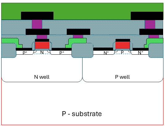
CMOS Process Steps: 3um to 1.25um
CMOS chips are made using a twin-well process, with precise tailoring of each well starting from a lightly doped substrate. Key production steps include using advanced masks, growing silicon oxide and nitride layers, ion implantation for wells, and using the LOCOS technique to isolate chip regions efficiently.