
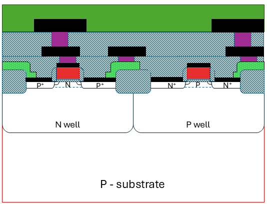
CMOS Process Steps: 3um to 1.25um
CMOS chips are made using a twin-well process, with precise tailoring of each well starting from a lightly doped substrate. Key production steps include using advanced masks, growing silicon oxide and nitride layers, ion implantation for wells, and using the LOCOS technique to isolate chip regions efficiently.
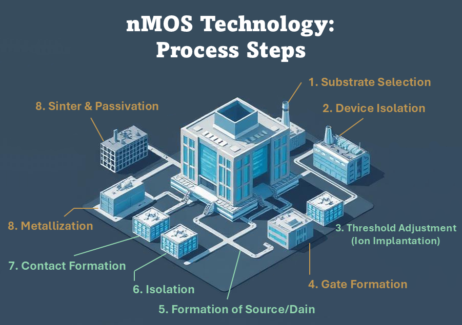
Basic nMOS Technology: Process Steps
NMOS fabrication involves key process steps like substrate selection, isolation, gate formation, and metallization. LOCOS isolation prevents unwanted current flow, while polysilicon gates enhance process stability. Ion implantation controls threshold voltage, ensuring device performance. Learn how NMOS advancements shaped microelectronics until CMOS became the preferred technology.