

This article is part of a series on the technology of integrated systems. We began with NMOS fabrication processes, but due to the fact that these were not power efficient, it quickly transitioned to CMOS technology, which offered almost no leakage current. In that post, we explained how CMOS devices are built—from start to finish. This current post focuses on scaling CMOS devices and the challenges that arise in doing so. The final two articles cover two key eras in integrated system technology: the microelectronics era (from 1 μm to 0.1 μm), and the nanoelectronics era (< 100 nm). In the former, scaling remains possible—though increasingly difficult. In the latter, we see that conventional MOSFETs no longer meet performance demands, prompting the need for entirely new device architectures.
Table of Contents
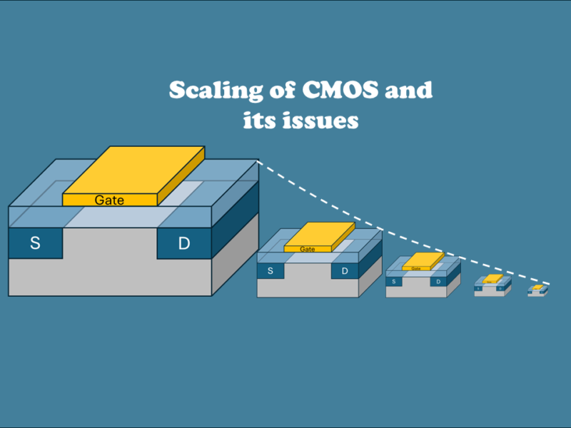
The incredible progress in the semiconductor industry has been fueled by one key principle: scaling. By making devices smaller, we’ve been able to pack more—and faster—transistors onto a single chip, driving advances in computing, communication, and everyday electronics. What began with feature sizes around 10 micrometers in the 1970s has evolved into today’s nanometer-scale technology. Several key enablers have made this scaling possible:
- Physics – A scaled MOSFET still behaves like a MOSFET, preserving its fundamental operating principles even at smaller dimensions.
- Materials – Silicon (and silicon dioxide) has been a foundational material. It has excellent semiconductor properties, forms a stable oxide, and allows the integration of new silicon-based materials, such as silicides.
- Technology – The MOSFET began as a 2D planar device, where the in-plane dimensions (width W and length L) control the current. Lithography advancements have been crucial in shrinking these dimensions. Vertical dimensions, such as layer thicknesses that influence threshold voltages, have been controlled through advanced deposition techniques like Atomic Layer Deposition (ALD).
Basic MOS transistor operations
Before we delve into scaling and the challenges it brings, it’s useful to briefly recap how a MOS transistor works and what its limitations are. This will help in understanding Dennard scaling more clearly.
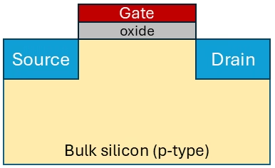
A MOS transistor has a gate terminal that controls the movement of electrons from the source to the drain through a silicon channel. The gate is separated from this channel by a thin layer of silicon dioxide, which acts as an insulator. Moreover, the source and drain regions are heavily doped with electrons (n-type doping). When the gate voltage is above a certain threshold voltage (VGS > Vth), a conducting channel forms, allowing electrons to flow. Conversely, when the gate voltage is below the threshold (VGS < Vth), the channel disappears, and current cannot flow. Importantly, the gate length defines the distance between the source and drain; in general, the shorter the gate, the faster the transistor can switch on and off.
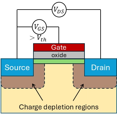
When a voltage is applied between the source and drain (VDS), the silicon bulk region near them becomes depleted of charge carriers. This happens because the source and drain are doped with one type of charge (e.g., electrons), while the bulk is doped with the opposite type (e.g., holes), leading to charge neutralization at the junctions. The depletion width depends on the doping concentration—higher doping results in narrower depletion regions.
As transistors shrink, the depletion regions of the source and drain can get close enough to overlap. When that happens, the gate loses some control over the channel, because the drain’s electric field starts influencing the channel directly. This causes the transistor to turn on more easily than it should, even when the gate is trying to keep it off—a phenomenon known as the short-channel effect. This effect becomes more pronounced when the drain voltage is increased, because a higher voltage widens the drain’s depletion region, further weakening the gate’s control.
Dennard Scaling
In 1974, Dennard and his colleagues proposed a scaling theory describing how transistor dimensions could be reduced proportionally while maintaining performance and energy efficiency. The core idea was that if the applied voltage (V) and all dimensions of a MOSFET—such as the channel length (L), width (W), and oxide thickness (tₒₓ)—shrink by a factor S, several predictable effects would occur. These effects are illustrated in Figure 3. In the text below, I highlight some of the key consequences of this scaling approach.
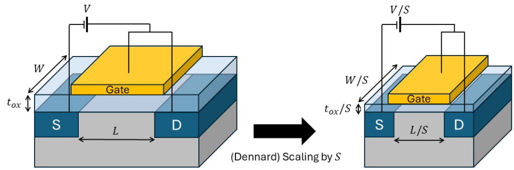
The gate capacitance depends on the area (width × length) and thickness, according to the following formula
\[C_{gate} = W\times L \times \frac{\varepsilon_{ox}}{t_{ox}} \ \rightarrow \ C_{gate}/S\]
As all these parameters scale with a factor S, the overall gate capacitance scales down by 1/S. This in turn has a direct impact on switching speed. The frequency of operation is inversely proportional to the RC time constant. So, when capacitance decreases, the frequency increases proportionally with scaling:
\[f=\frac{1}{R_{ON}C}\ \rightarrow\ f\times S\]
Not just the dimensions can be scaled, but also the applied voltage V. This has effect on the electric field inside the transistor (E = V/L). This electric field is essential for regulating the movement of charge carriers (electrons or holes) within the transistor. As both the gate length and the gate-source voltage, the electric field remains unchanged. Another critical aspect related to the applied voltage is the power consumption:
\[P = f\times CV^2 \ \rightarrow\ P/S^2\]
Since both capacitance and voltage scale down, the power consumed by each transistor decreases by 1/S2. Meanwhile, if the number of transistors that can fit in the same area increases by S2, it results in a constant power density.
What does NOT scale?
When they started implementing the scaling strategy as shown in the paper by Dennard et al., they found that the voltage and current scaled down almost perfectly. However, not all transistor parameters scaled down, such as the subthreshold slope and the interconnect resistance. This turned out to be one of the contributing factors to the end of Dennard scaling almost 30 years later.
Subthreshold slope
Ideally, when the gate-source voltage (VGS) is reduced below the threshold voltage (Vth), the transistor turns off completely, as illustrated in Figure 4 (left). However, in reality, even at voltages below the threshold, a small current—known as leakage current—still flows through the channel. This occurs due to the thermal excitation of charge carriers. This behavior becomes more apparent when observing the drain current (ID) on a logarithmic scale, as shown in Figure 4 (right).
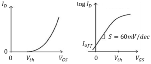
The rate at which the current increases as the gate-source voltage rises in the subthreshold region is known as the subthreshold slope. This slope does not scale, and can be mathematically calculated to be:
\[S_{threshold} = \frac{q}{kT} \approx 60 mV/dec\]
This means that for every 60 mV increase in VGS, the drain current increases by a factor of 10 (i.e., one decade), no matter the size of the transistor [5].
Interconnect resistance
Something that often gets overlooked are the interconnects—the tiny metal wires that connect transistors together. Unlike transistors, interconnects do not scale well. As transistors get smaller, so does the width of the interconnect lines. If the thickness of these metal lines stays the same, the cross-sectional area decreases, which causes the resistance of the interconnects to increase by a factor of S.
Now consider the RC delay of an interconnect, where R is resistance and C is capacitance. While resistance increases by S, the capacitance typically decreases due to reduced area and spacing, often by about 1/S. At first glance, this seems to balance out, keeping the RC delay constant:
\[\tau = RC\propto S\frac{1}{S}=\text{constant}\]
However, here’s the problem: transistor switching speeds increase with scaling—by roughly the same factor S. That means to keep up, interconnects must become faster, not stay the same. So even if the RC delay doesn’t get worse, it becomes a relative bottleneck compared to faster transistors [6].
Problems when scaling down
With technological advancements, it became possible to fabricate transistors with increasingly smaller feature sizes. However, scaling down the supply voltage proved to be challenging. In an ideal scenario—referred to as constant electric field scaling—both voltage and dimensions are reduced proportionally. This would result in extremely low voltages at advanced nodes; for instance, a supply voltage of 80 mV and a threshold voltage of just 1.3 mV at a feature length of 0.1 μm, as illustrated in Figure 5. Such values are impractical, primarily because the subthreshold slope does not scale accordingly.
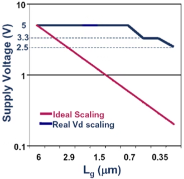
Instead, the industry adopted a (quasi) constant voltage scaling approach, where the supply voltage remained unchanged over several technology generations. For example, it was maintained at 5 V until the gate length reached approximately 0.7 μm. As shown in Figure 5, the supply voltage was then gradually reduced in discrete steps—plateaus—driven by reliability concerns, some of which I will discuss in the following sections. The main issue that has to be understood from this section is that by keeping the voltage constant, but reducing the length of the minimum feature by scaling it down, increases the electric field.
Punch-Through
One of the early challenges with constant voltage scaling was the emergence of punch-through as channel lengths decreased. In long-channel MOSFETs, the gate exerts strong control over the channel, and the source and drain depletion regions remain well separated. As a result, even relatively high drain voltages (e.g., 5 V) do not lead to punch-through. However, in short-channel devices, the same drain voltage can cause the depletion regions to extend further into the substrate, potentially merging. This reduces the gate’s control and allows unintended current to flow directly from drain to source — a phenomenon known as punch-through. Figure 6 illustrates the merging of the two depletion regions.
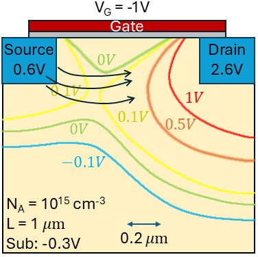
To mitigate this, anti-punchthrough ion implantation is used. This technique introduces dopants in a confined area just beneath the channel to suppress the merging of depletion regions. The localized nature of this implant helps limit leakage while preserving overall device performance.
Velocity Saturation
In addition to punch-through, high electric fields in short-channel devices also lead to velocity saturation. At low electric fields, carrier velocity increases linearly with the field. However, once the field exceeds a certain threshold (typically around 10⁴ V/cm for electrons in silicon), the carriers reach a maximum drift velocity — known as the saturation velocity. Beyond this point, increasing the electric field no longer results in faster carrier motion, which limits the drain current (ID) and overall transistor performance.
In the long-channel transistor operation, in saturation, the drain current ID increases quadratically with gate voltage:
\[I_D \propto (V_{GS}-V_{th})^2\]
However, in short-channels MOSFETs with high electric fields — the carriers can’t accelerate any further. Their drift velocity saturates, and becomes linear and results in:
\[I_D \propto V_{GS} -V_{th}\]
![Fig 7. I-V characteristics of long- and a short-channel NMOS transistor. Observe the difference in y-axis scale. Image taken from [2].](https://florisera.com/wp-content/uploads/2025/04/velocity-saturation.avif)
Ideally, the drain current should remain constant when scaling down both the transistor dimensions and supply voltage. However, as the channel length decreases, electric fields increase, leading to velocity saturation. This effect limits the carrier drift velocity, reducing the available current. This trend is evident in Figure 7, where the drain current is reduced by by 56% when looking for VGS = 2.5 V and VDS = 2.5 V (0.54mA versus 0.22mA).
Hot Carrier Effects (HCE)
The hot carrier effect emerged as a reliability concern in MOS transistors as devices were scaled down and electric fields increased. When carriers (electrons or holes) accelerate from source to drain under high electric fields, some gain enough kinetic energy to become “hot.” These energetic carriers can inject into the gate oxide or become trapped, causing threshold voltage shifts, transconductance degradation, and long-term device instability.
When examining Figure 8, we see the hot carrier lifetime (in seconds) plotted for various technology nodes ranging from 0.7 μm to 0.18 μm. The x-axis shows the inverse of the drain voltage (1/VD) , so higher drain voltages appear on the left, and lower voltages on the right. For each technology node, reducing the drain voltage leads to a significant increase in transistor lifetime.
This clear dependence of lifetime on operating voltage was a key factor in supply voltage scaling. As transistor gate lengths approached 0.7 μm, the standard operating voltage dropped from 5V to 3.3V, and continued to decrease in steps.
![Fig 8. Lifetime of transistor devices for technologies from 0.7 um to 0.18 um. Image taken from [3].](https://florisera.com/wp-content/uploads/2025/04/hot-carrier-lifetime-768x598.png)
In addition to reducing the supply voltage, further measures were taken to lower the electric field within the transistor. Abrupt drain junctions were found to worsen the hot carrier effect by concentrating the electric field near the drain. To address this, special techniques, such as lightly doped drain (LDD) structures, graded junctions, and deep drain diffusions (DDD) were implemented. These modifications help spread out the electric field, reducing peak intensities, slowing carrier acceleration, and ultimately minimizing hot carrier-induced damage.
Time Dependent Dielectric Breakdown (TDDB)
Another important mechanism that impacted the transistor reliability is time-dependent dielectric breakdown. This is related to the gradual degradation of the dielectric material (such as the insulating silicon oxide layer) due to sustained voltage stress. Over time, the dielectric layer weakers and it breaks down, allowing current to flow through it. This causes permanent damage to the device, effecting its ability to insulate and leads to failure.
Improvement in the oxidation technology and screening helped preventing this breakdown. Also the use of alternative dielectrics helped, and we will get back to this in a future post when talking about transistors in the 1 μm to 100 nm range (the microelectronics era).
Ultimate Scaling Limitations
Of course, scaling cannot be done inifinitely, as at some point you reach the physical limits. I.e. when the oxide thicknessscales below a few nanometer, quantum mechanical effects occur. There are technological limitations as well, where the line edge roughness doesn’t scale at the same pace as the dimensions, this causes device variability.
However, one of the main problems is the dopant concentration variability. In small volumes, small concentrations result in large statistical variations. F.L. Yang et al. showed that discrete dopants randomly distributed in a ~100 nm3 cube. Dopants inside the sub-cubes are ranged from 7 to 27 with average number of 17 and. This variability becomes an important issue, when creating source and drain areas, as it could be different for different MOSFETs
![Fig 9. Doped (105 nm^3) cubed, with 343 sub-cubes. Dopants inside the sub-cubes are ranged from 7 to 27, with average number of 17 and one standard deviation of 4. Image taken from [4].](https://florisera.com/wp-content/uploads/2025/04/variability.avif)
Reference
[1] S. Perlot, Finding the Next-Moore’s law in Future Compute Systems, 2023. Available: https://medium.com/@steelperlot/finding-the-next-moores-law-in-future-compute-systems-05c492a42762 [Accessed: April 2025].
[2] CMOS Technology Scaling. Available: https://pdfs.semanticscholar.org/presentation/ d1c4/843de0863c64ee49 44d035fc2027ea7268b7.pdf [Accessed: April 2025].
[3] Available: https://ui.adsabs.harvard.edu/abs/1982ITED…29..611T/abstract [Accessed: April 2025].
[4] F.L. Yang, “Outlook for 15nm CMOS research technologies” in 2010 10th IEEE International Conference on Solid-State and Integrated Circuit Technology, November 2010, Shanghai, China. IEEE. Available: https://sci-hub.se/10.1109/ICSICT.2010.5667850 [Accessed: April 2025].
[5] Van Overstraeten, R. J., Declerck, G., & Broux, G. L. (1973). Inadequacy of the classical theory of the MOS transistor operating in weak inversion. IEEE Transactions on Electron Devices, 20(12), 1150–1153. doi:10.1109/t-ed.1973.17809
[6] Saraswat, K. C., & Mohammadi, F. (1982). Effect of scaling of interconnections on the time delay of VLSI circuits. IEEE Transactions on Electron Devices, 29(4), 645–650. doi:10.1109/t-ed.1982.20757
Other references
Florius
Hi, welcome to my website. I am writing about my previous studies, work & research related topics and other interests. I hope you enjoy reading it and that you learned something new.
More Posts