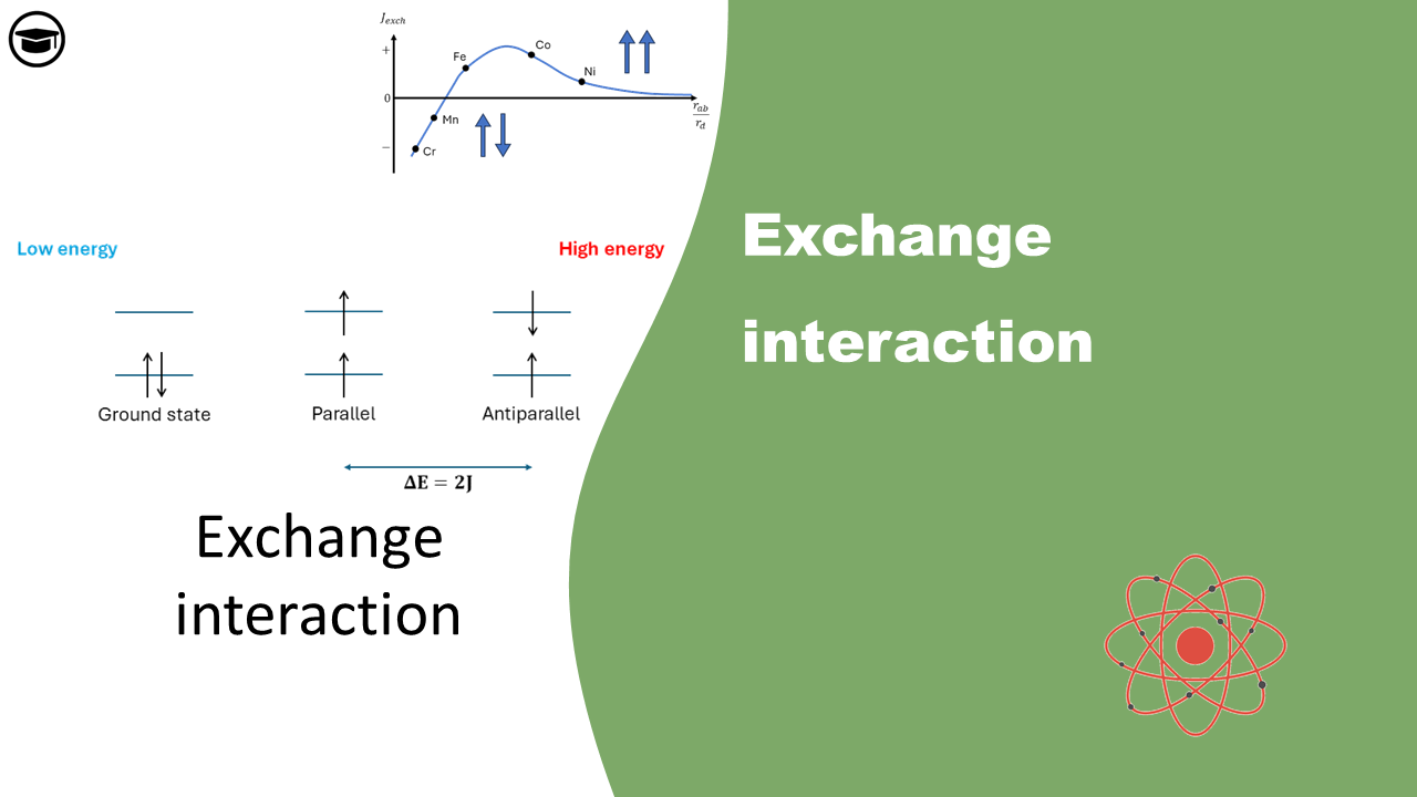
Overheating batteries are a serious risk, in the worst cases leading to fires and explosion. A team has now developed a simple, cost-effective method to test the safety of lithium-ion batteries, which opens up opportunities for research into new and safer batteries for the future. The researchers created an intentionally unstable battery which is more […]
Scientists have repurposed smartphone camera sensors to create a detector capable of tracking antiproton annihilations in real time with unprecedented resolution. This new device can pinpoint antiproton annihilations with a resolution of about 0.6 micrometers, a 35-fold improvement over previous real-time methods.
Engineers have designed and synthesized a groundbreaking new material -- a copper-free superconducting oxide -- capable of superconducting at approximately 40 Kelvin, or about minus 233 degrees Celsius, under ambient pressure.
Imagine navigating a virtual reality with contact lenses or operating your smartphone under water: This and more could soon be a reality thanks to innovative e-skins. A research team has developed an electronic skin that detects and precisely tracks magnetic fields with a single global sensor. This artificial skin is not only light, transparent and […]
Crashes on electric scooters are mostly due to the behavior of the riders, with one-handed steering and riding in a group being some of the largest risk factors. The researchers are also concerned about riders who deliberately crash or cause dangerous situations when riding, a phenomenon that seems to be specific to electric scooters.
This a robot can walk, without electronics, and only with the addition of a cartridge of compressed gas, right off the 3D-printer. It can also be printed in one go, from one material.
In this article I will discuss what thyristors are and how they work. I will start with the semiconductor structure of a thyristor and use the characteristic V-I curve to explain the three different modes. Subsequently, I will use an two transistor model to explain the thyristor from a different point of view. Lastly, I will briefly explain how to turn off typical silicon controlled rectifiers. [latexpage]
1. Thyristors
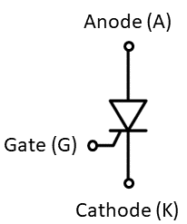
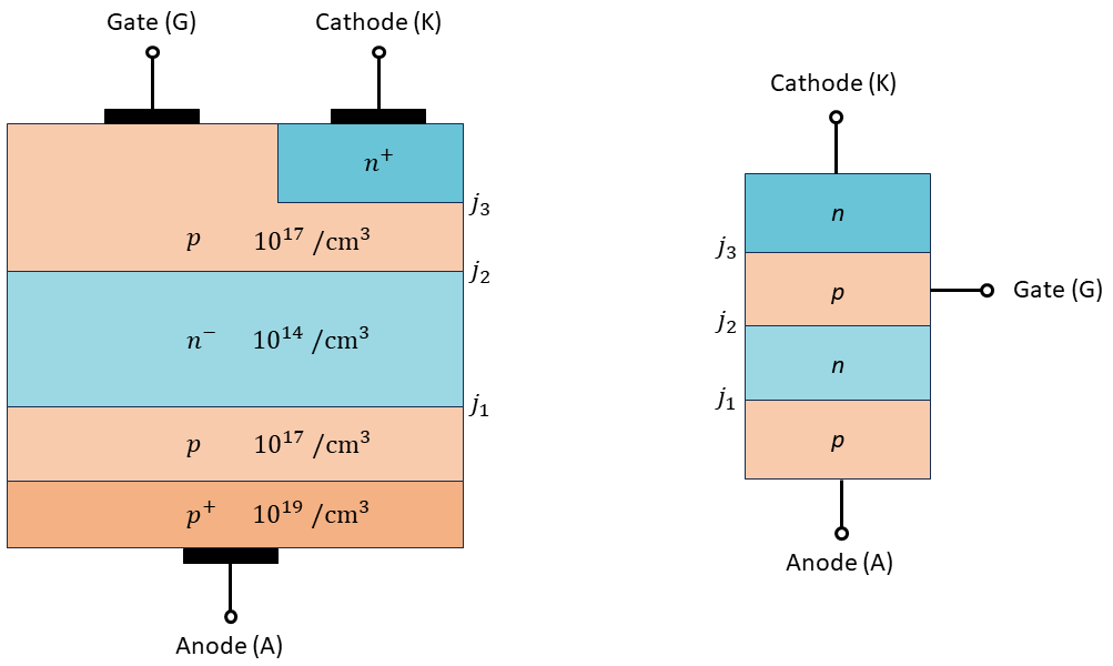
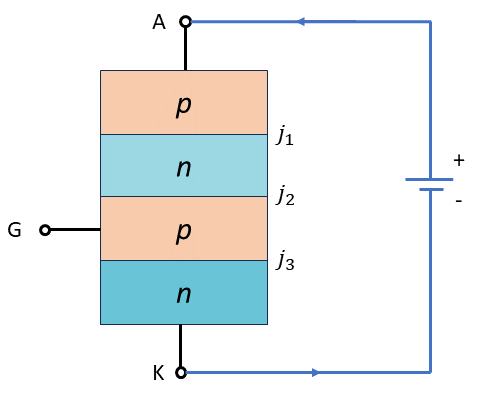
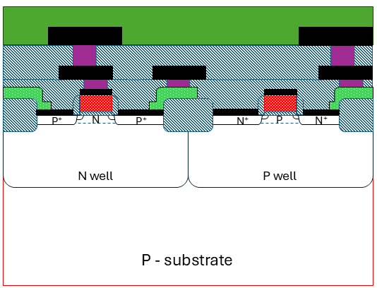
Thyristors are four layer devices, with three terminals: Anode (A), Cathode (K) and Gate (G). Figure 2 shows an illustration of the structure of a thyristor. The anode is formed from the p and p+ layers. The thickness of this part is roughly 30 to 50 μm. The n– layer is only lightly doped compared to the rest, with a doping level of around 1014 cm3. However the width is ranging from 50 to 1000 μm. When the thyristor is forward biased (meaning VAK is positive), the junction j2 is reversed biased and the other two junctions are forward biased. The depletion layer formed at j2 is absorbed by the n– layer. The width corresponds to the forward blocking voltage of the thyristor.
The other p layer is doped at around 1017 cm3 and forms the gate of the thyristor. The last n+ layer has a doping of 1019 cm3 and forms the cathode. In the next sections, I will explain the workings of this device with the different modes.
Fig 2. Thyristor NPNP construction
On the right hand side of Figure 2 is the simplified structure of the thyristor. This figure is what you will find in most articles on thyristors, but remember that this is only a simplified figure of the left hand side.
Some might confuse a thyristor with a power diode, but they are not exactly the same. A thyristor has a gate terminal that can control the device, and because of the extra layer(s), it also has more junctions than a diode (which has only 1 junction). While diodes are used for rectification, freewheeling and feedback; thyristors are mainly used for controlled rectification AC regulation, inversion and DC-DC conversion. Furthermore, diodes are used as protection for thyristors.
The advantages of thyristors:
Only a small amount of gate drive is required, since it is a regenerative device.
They exist with high voltage and high current ratings.
ON-state losses are reduced in thyristors.
The disadvantages of thyristors:
Once the thyristor is on, the gate no longer has control over it (however, special GTO-thyristors exist which are fully controllable by the gate terminal).
external circuits are required to turn it off.
2. Characteristics of thyristors
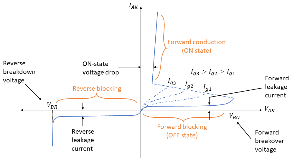
The working of a thyristor can be discussed in three different modes, namely the reverse blocking mode, the forward blocking mode and the forward conducting mode. Figure 3 shows the static V-I characteristic of a thyristor. The anode to cathode current (IAK) is plotted against the anode to cathode voltage (VAK). Furthermore, there is a reverse breakdown voltage (VBR) and a forward breakover voltage (VBO). Different gate currents (i.e. Ig1 , Ig2, Ig3) can be applied to the thyristor.
Fig 3. Thyristor VI curve
2.1 Reverse blocking mode
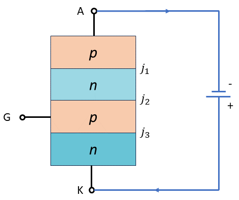
Figure 4 shows the situation when a thyristor is in reverse blocking mode. The anode (A) is made negative with respect to the cathode (K) (negative VAK). The gate terminal (G) is kept open. Due to the PN layering, there are 3 junctions, j1, j2, j3. Out of these 3 junctions, j1 and j3 are reverse biased, and j2 is forward biased. Only junction j2 is in forward bias. Because of the reverse bias, the thyristor does not conduct,. However, there is still a very small current flowing from the cathode to the anode, which is called the reverse leakage current.
As can be seen by Figure 3, in this reverse blocking mode, the voltage can increase (to the left), but only small amount of current flows. At a certain voltage, called the reverse breakdown voltage (VBR), the reverse current increases dramatically. At this moment, with high voltage and high current, there is a large power dissipation in the thyristor. Because of that, the thyristor’s junction temperature has exceeded its specified limit and it will break down. That is why reverse voltage should never exceed VBR!
Fig 4. Reverse biased thyristor
I mentioned that the gate terminal is kept open during reverse blocking mode. If you’d apply a positive voltage on the gate and cathode, junction j3 is forward biased. Now j3 and j2 are both forward biased, and more leakage current will flow, adding to the dissipation.
2.2 Forward blocking mode
Figure 5 shows the situation when a thyristor is in forward blocking mode. The anode is made positive with respect to the cathode (positive VAK). Because of this configuration, junctions j1 and j3 are now forward biased and j2 is reverse biased. That means, that the forward voltage is still on hold by the junction j2. A small current still flows, called the forward leakage current. In this mode, the thyristor is forward biased, but it does not turn on. You can increase the voltage up to the forward breakover voltage (VBO), and once it reaches it, the thyristor turns on (it won’t get damaged unlike at the VBR side). At this stage, it goes from forward blocking to forwarding conducting mode.
The forward breakover voltage is obtained due to the blocking capability of junction j2, while the reverse blocking capability is due to junctions j1 and j3 combined. Because the latter is stronger than just junction j2; the reverse blocking voltage is higher than the forward blocking voltage of a thyristor.
Fig 5. Forward biased thyristor
2.3 Forward conducting mode
There are several techniques for which the thyristor can go from forward blocking mode to forward conduction mode:
When VAK > VBO
When voltage is applied to the gate terminal
When the gate-cathode junction (j3) is exposed to light
when dv/dt exceeds its specified limits
1. VAK > VBO
When VAK > VBO , the thyristor is driven in forward conduction mode, no matter the voltage on the gate (even if grounded). As mentioned before, during the forward blocking mode, junction j2 is in reverse bias, but when VAK gets too large, avalanche breakdown of the junction takes place, and a large current flows through the thyristor and the voltage between anode and cathode reduces to a small value. This current is limited to the external load in the system, hence: IAK = V/Load
2. Gate triggering
A positive gate voltage is applied with respect to the cathode, and it drives the thyristor from forward blocking mode into forward conducting mode. When this voltage is applied, an additional current starts flowing in parallel to the forward leakage current. The avalanche breakdown at junction j2 now requires less VAK voltage to start. The thyristor can be brought into forward conduction mode below VAK < VBO , as is shown in figure 3 by the dashed lines Ig1 , Ig2, Ig3. As the gate current increases, the lower the anode to cathode voltage is. Once the thyristor goes into forward conducting mode, the gate has no control over the conduction, and the current is limited similar to what was discussed before.
3. Light activated SCR
Similar to part 2, but instead of putting a voltage on the gate, if the gate-cathode junction, j3, is exposed to a beam of light, current starts to flow due to the photons of light. This current drive the thyristor into conduction. These systems are a special type of thyristor, called the Light activated Silicon Controlled Rectifier (LASCR).
4. dv/dt exceeds limits
During the forward blocking mode, a small forward leakage current flows through the thyristor; and something equivalent to an internal capacitor is formed inside the thyristor; one from anode to gate and the other from gate to cathode. A transient current can be induced in these internal capacitors by rapid changes in the voltage across the thyristor. This current adds to the foroward leakage current, and similar to gate triggering, it lowers the anode to cathode voltage required to turn it on. It can trigger the thyristor at unwanted moments, and to avoid that, you must keep the voltages changes below its permissible value, given in the datasheet. One way to stop this, is by adding a small resistance between gate and cathode that acts as an external path for this transient current.
2.4 Latching current vs Holding current
In thyristors, specifically in the context of silicon-controlled rectifiers (SCRs), the terms “latching current” and “holding current” refer to two important operating parameters. The definitions appear similar, but they are very different. I will try to explain their differences below:
Latching current is effective at the time the thyristor turns ON, whereas the holding current is effective at the time it turns OFF.
Latching current is the minimum current that is required at the time of triggering to turn ON the thyristor. Whereas once the thyristor is already in the ON state, it current should not be below the holding current, otherwise it turns OFF.
Lastly, Latching current is always greater than Holding current.
2.4.1. Calculation example
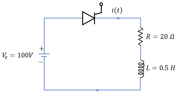
Fig 6. Thyristor example
In this example, the thyristor has a latching current of 20 mA (it requires 20 mA to turn on), and is fired with a pulse of 50 μs. We will see if the current is large enough to turn on the thyristor.
The current through the RL circuit for a step input is given as:
The current through the thyristor is only 10 mA, and does reach the latching current required to turn on the thyristor. One possible way, is to increase the width of the pulse to increase the current.
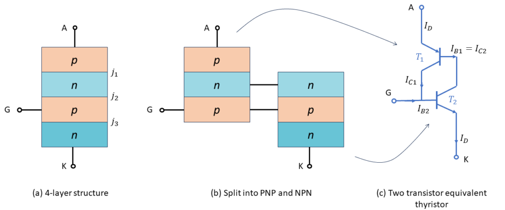
3. Equivalent two transistor model
Using the two transistor model is a good way to explain a thyristor. Figure 7 shows how to convert a 4 layer structure (a) into a two transistor model (c).
Fig 7.
When you have a 4-layer thyristor, you can imagine the top 3 layers and the bottom 3 layers as separate parts. Each part is a transistor; transistor T1 is pnp, while transistor T2 is npn. The base of T1 is connected to the collector of T2. Similarly, the base of T2 is connected to the collector of T1. Both of these transistors are in common base configuration. When the thyristor is forward biased, and the gate is left open, the current ID flows from anode to cathode. Current ID is a combination of collector current, emitter current and leakage current of both transistors combined.
Through some mathematics, you can conclude that the current ID can be calculated by:
where (ICO1 + ICO2) are the total reverse leakage currents of the junction j2. α1 and α2 are common base gains of transistor 1 and 2, respectively. Initially they are small, but when the forward voltage increases, the gains also increase. When it reaches unity, ID goes to infinity. This is the moment the thyristor goes to forward conduction mode, and the current is only limited by the external load.
4. Turning off
Now that we know how a thyristor works, it might be beneficial to also know how to turn it off. There are special Gate Turn Off thyristors, but in this last chapter I briefly want to focus on the normal silicon controlled rectifier and how to turn it off.
We know that a thyristor turns off when the current falls below the holding current, this can be done by either natural or forced commutation. For natural commutation, you lower the supply voltage; or even go negative, this will put the thyristor in reverse bias. With forced bias, additional external components can temporarily apply an impulse of negative current turning it off as well. This external circuitry has to create an impulse of a certain duration to let the excess carriers near junction j2 recombine. This time is called gate recovery time (tgr). If the impulse is shorter than this, the thyristor may turn on again.
Hi, welcome to my website. I am an electronic enthusiast, writing about my previous studies, work & research related topics and other interests. I hope you enjoy reading it and that you learned something new.