A study describes a new method of recycling silicone waste (caulk, sealants, gels, adhesives, cosmetics, etc.). It has the potential to significantly reduce the sector's environmental impacts. This is the first universal recycling process that brings any type of used silicone material back to an earlier state in its life cycle where each molecule has […]
If you haven't heard of a tardigrade before, prepare to be wowed. These clumsy, eight-legged creatures, nicknamed water bears, are about half a millimeter long and can survive practically anything: freezing temperatures, near starvation, high pressure, radiation exposure, outer space and more. Researchers took advantage of the tardigrade's nearly indestructible nature and gave the critters […]
Engineers developed a technique to grow and peel ultrathin 'skins' of electronic material that could be used in applications such as night-vision eyewear and autonomous driving in foggy conditions.
Researchers have demonstrated a significant performance increase in cooling technology for high-power electronic devices. They designed novel capillary geometries that push the boundaries of thermal transfer efficiency. This study could play a crucial role in the development of next-generation technology.
Switching from diesel to electric trains dramatically improved the air quality aboard the San Francisco Bay Area's Caltrain commuter rail line, reducing riders' exposure to the carcinogen black carbon by an average of 89%, finds a new study. The electrification of the system also significantly reduced the ambient black carbon concentrations within and around the […]
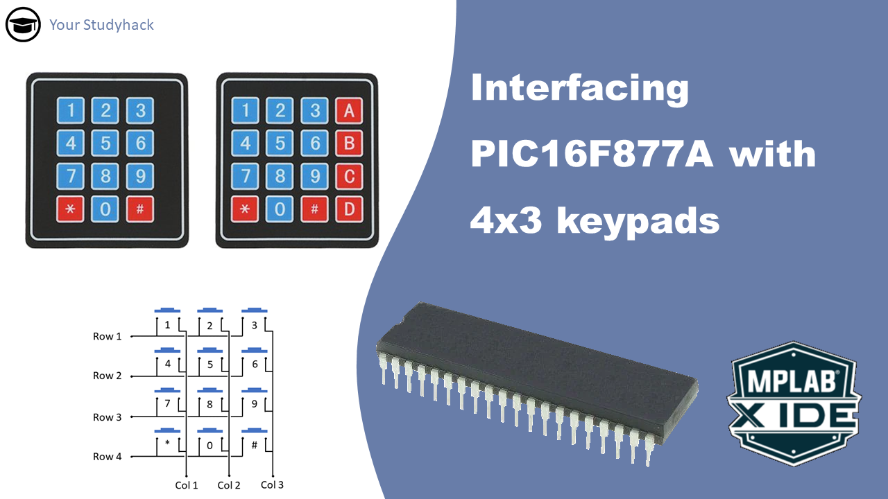
In this tutorial, we will provide an overview of the 4×3 membrane keypad. The keypad serves as a reliable and budget-friendly tool for having inputs in your project. Understanding how to interface with the keypad will prove useful in future projects that require menu selection or similar inputs. Our guide intends to provide a comprehensive understanding of the the basics of the 4×3 membrane keypad. Through this, you will gain valuable insight that will help you in your projects.
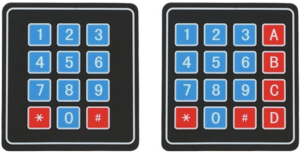
Membrane keypads are available in various sizes, including the widely used 4×3 keypad with 12 keys (0-9 with 2 symbols), and the 4×4 keypad with 16 keys (0-9, A-D and 2 symbols). These keypads are designed in a standard telephone keypad layout which makes them user-friendly for everyone.
Fig 1. Keypad of 4x3 and 4x4 sizes.
1. The layers of a membrane keypad
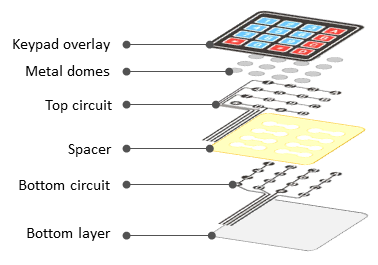
The membrane keypad is made with flexible materials making it ideal for use on a variety of surfaces, including curved ones. As illustrated in Figure 2, the keypad is comprised of multiple layers. The topmost layer, the keypad overlay, functions as a visual interface similar to that of conventional telephones. Directly below it lies a layer of metal domes that provide tactile feedback upon button activation. The following three layers serve to create a complete circuit. At the top circuit, a voltage is applied, and a spacer separates it from the bottom circuit when the button is not pushed. Upon activation, the top circuit connects with the bottom circuit, completing the entire circuit. Finally, the bottom layer acts as a seal, enclosing the entire package.
Fig 2. The different layers of a membrane keypad.
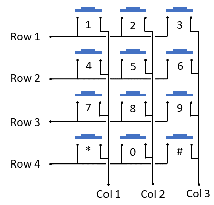
Because the complete circuit is made by connecting a row with a column, for the 4×3 keypad, only 7 I/O connections are required for a total of 12 different inputs. The 4×4 keypad, as depicted in Figure 2, requires only 8 connections for 16 different inputs.
2. Membrane keypad scanning
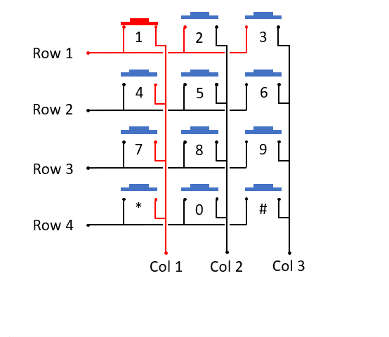
As shown in the previous section, the keypad consists of 12 (or 16) buttons, that can be pushed down; which basically acts as a switch between the row and columns. To illustrate, take a look at Figure 3. The leads to button “6” are connected to Row 2 and Col 3. If button “6” is pushed down, and Row 2 is pulled high, this can be seen on Col 3 as there is a direct connection. The other two columns will stay grounded and no input is seen on those.
Fig 3. Illustration of the 12 buttons on the keypad, with their connections.
Here is how a keypad works with a microcontroller:
Each row of the keypad is connected to an output pin of the microcontroller.
All columns of the keypad are connected to the input pins of the microcontroller.
The columns are normally pulled low by pull-down resistors (either external or internal).
The output rows are all set to low.
If the input pins measure low, the buttons are not activated.
The microcontroller starts sequencing through the rows, setting them high one by one.
If any of the buttons is pressed, the corresponding row will be pulled high. This will also cause the corresponding column input to go high.
The microcontroller can then read the column input to determine which button is pressed.
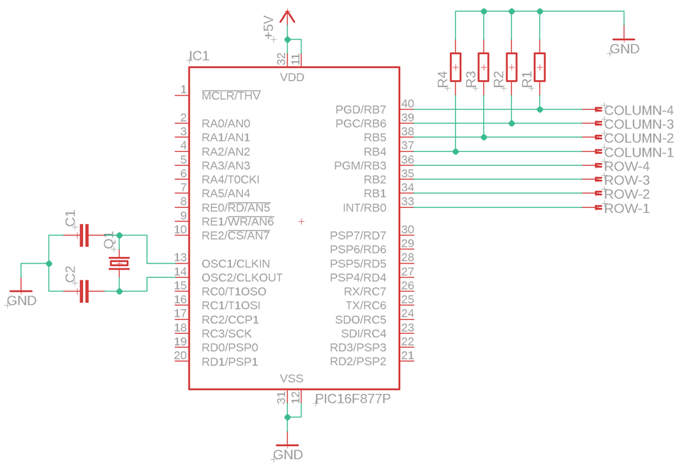
3. Connecting 4x3 and 4x4 keypad to a microcontroller
The following figures demonstrate a straightforward connection process. However, it is essential to emphasize that the exact pin diagram of the keypad varies by maker, always do check with the datasheet of your own keypad. But in nearly all cases, the first 4 buttons on the left correspond to the Rows (R1, R2, R3, R4), and the 3 buttons on the right correspond to the columns (C1, C2, C3).
Assuming a PIC16F877A microcontroller is being used and a 4×3 matrix keypad, you may omit Column 4 (C4). Pins RB0 to RB3 must be set as output as they connect to the four rows, whereas pins RB4 to RB7 can be set as inputs. In addition, all columns have a pull-down resistor to obtain a proper ground on the inputs. This can also be accomplished through internal pull-down resistors inside the microcontroller. If this programmed it like that, you can entirely eliminate external pull-down resistors.
4. Microcontroller example code
The following is an example code where I made a scanKeypad function. The function utilizes a loop to make only one row high per iteration, and subsequently checks the columns for any button press. Please note that determining the use of the function’s return value rests with the user, and you can do anything with it. If you want to display this number on an LCD screen, please check my other page on interfacing with LCD.
					#include <xc.h>
#define _XTAL_FREQ 20000000 // Define crystal frequency to 20 MHz

// Configuration bits
#pragma config FOSC = HS
#pragma config WDTE = OFF
#pragma config PWRTE = OFF
#pragma config BOREN = OFF
#pragma config LVP = OFF


char scanKeypad() {
    char row, col;
    const char keypad[4][3] = {
        {1, 2, 3},
        {4, 5, 6},
        {7, 8, 9},
        {'*', 0, '#'}
    };

    // Loop through each row
    for (row = 0; row < 4; row++) {
        PORTB = (PORTB & 0xF0) | (1 << row); // Set only the specified row bit
        __delay_ms(10); // Delay for debounce

        // Read the column inputs, set them to the lower nibble first and mask them with 0b00000111
        col = (PORTB >> 4) & 0x07;

        if (col == 0x01 || col == 0x02 || col == 0x04) {
            return keypad[row][col]; // Return keypad value
        }
    }
    return -1; // Invalid col value (multiple same time) or no button pressed
}

void main() {
    // Initialize ports
    TRISB = 0xF0; // RB0 - RB3 as output (rows), RB4 - RB6 as input (columns)
    PORTB = 0x0F; // Set initial output values for rows to low, and enable weak pull-ups for column inputs
    char buttonPressed;

    while (1) {
        buttonPressed = scanKeypad(); // Performs a scan of the keypad

        if (buttonPressed != -1) {
            // A button is pressed! Look at my LCD page to find more on how to display it:
            // https://florisera.com/embedded-systems/connecting-pic16f877a-with-an-lcd-screen/
        }
    }
}
5. Summary
In this tutorial we have seen the workings of a keypad membrane by providing a detailed examination inside by corresponding illustrations. It also offers guidance on interfacing the keypad with the PIC16F877A microcontroller using both a pin diagram and program code.
Post Views:245
Florius
Hi, welcome to my website. I am writing about my previous studies, work & research related topics and other interests. I hope you enjoy reading it and that you learned something new.