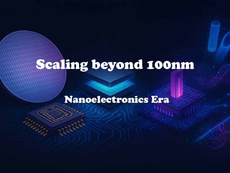

Scaling beyond 100nm – Nanoelectronics Era
As silicon and silicon dioxide reach their scaling limits, engineers turn to high-k materials, metal gates, and new device architectures like FinFETs and SOI. These advances define the nanoelectronics era. Yet even FinFETs have limits—pushing research toward carbon nanotube FETs, tunnel FETs, and spin-based devices that could drive future breakthroughs.
Scaling of CMOS: Microelectronics era
As CMOS technology shrank below 1 μm in the microelectronics era, high electric fields caused reliability issues like hot carrier effects. Techniques such as LATID and Anti-Punch Through (APT) were introduced to control these effects and extend the performance of shrinking devices.
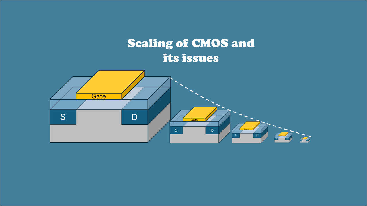
Scaling of CMOS and its Issues
Dennard scaling revolutionized microelectronics by showing that reducing transistor size and voltage proportionally keeps power density constant. However, real-world limitations like subthreshold slope and interconnect resistance eventually halted its ideal progression, demanding alternative approaches to maintain performance improvements in modern technology nodes.
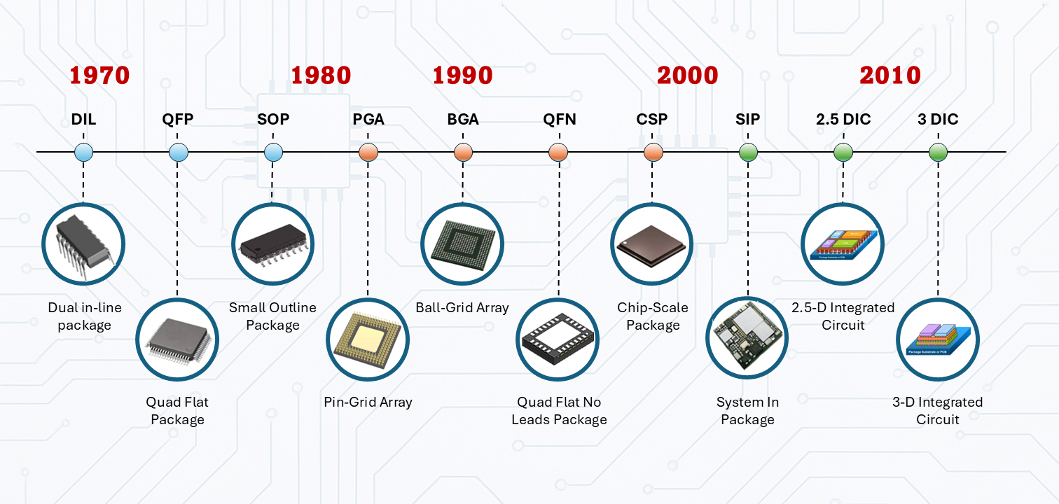
CMOS Process Steps: 3um to 1.25um
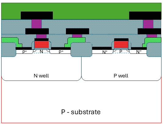
CMOS chips are made using a twin-well process, with precise tailoring of each well starting from a lightly doped substrate. Key production steps include using advanced masks, growing silicon oxide and nitride layers, ion implantation for wells, and using the LOCOS technique to isolate chip regions efficiently.
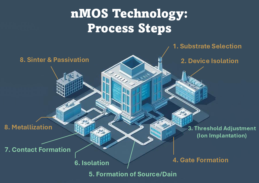
Basic nMOS Technology: Process Steps
NMOS fabrication involves key process steps like substrate selection, isolation, gate formation, and metallization. LOCOS isolation prevents unwanted current flow, while polysilicon gates enhance process stability. Ion implantation controls threshold voltage, ensuring device performance. Learn how NMOS advancements shaped microelectronics until CMOS became the preferred technology.
The Physics and Technology of Extrinsic Semiconductors
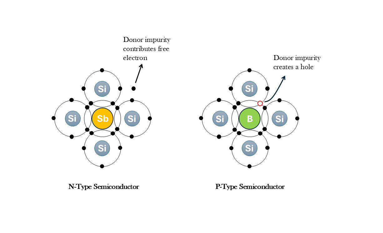
Doping modifies a semiconductor by introducing donor or acceptor atoms, increasing free electron or hole concentration. This creates an n-type or p-type material, shifting the Fermi level closer to the conduction or valence band, respectively. The level of doping determines electrical conductivity and charge carrier behavior.

The Physics and Technology of Intrinsic Semiconductors
Semiconductors are materials with electrical properties between metals and insulators, governed by their band structure. The valence and conduction bands define electron movement, with a band gap influencing conductivity. Intrinsic semiconductors, free of impurities, require energy to excite electrons into the conduction band, enabling current flow. Carriers, including electrons and ...
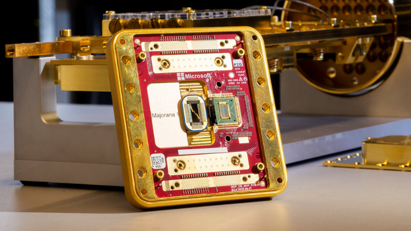
Majoranas: The Next Step in Quantum Computing
Microsoft’s Azure Quantum team is developing quantum chips using topological qubits, leveraging Majorana zero modes for stability. Their research on superconducting nanowires could accelerate quantum computing advancements. This article explains Majorana physics, its role in quantum systems, and Microsoft’s roadmap for scalable quantum computing, offering insights into this groundbreaking development.

Beyond Conductivity: Advanced Metal Science
Explore the advanced physics of metals beyond conductivity. Learn about superconductivity, AC conductivity, and electromagnetic interactions.

The Physics and Technology of Metals
Understanding the conductivity of metals involves exploring their high electron mobility, Ohm’s law, and quantum mechanical models like Drude and Sommerfeld. This article discusses how metals conduct electricity, the role of energy bands, and how electron interactions shape conductivity, highlighting key concepts like drift velocity, Fermi energy, and relaxation time.