
1. superconductivity
Superconductivity was first discovered in 1911, in Holland, by H, Onnes. He discovered that when you look at the conductivity of Mercury, the resistivity drops below a certain temperature, to where it looks like there is no more resistivity anymore. These kind of materials where coined “superconductors (SC)”. For a very long time, this wasn’t so interesting, as it happened at very low temperatures.
It took until the 1980’s, when ceramic materials having critical temperatures above 77 K were synthesized, which were called “high-Tc superconductors”, due to the fact their critical temperature was above the boiling temperature of liquid Nitrogen. It was in 1987 that two physicists, Bednorz and Müller received the Nobel prize for their important breakthrough in the discovery of superconductivity in ceramic materials. After this, it became a hot topic, and many researchers started studying, and they all wanted to get the holy grail of superconductivity, “superconductors at room temperature”. However, material science doesn’t work like that. Several classes of SC were found, and large breakthroughs were made, but they all flattened off far below room temperature.
1.1 Cooper pairs
Superconductivity results from an instability in the Fermi liquid ground state arising from an effective attractive interaction between the electrons. This attraction comes about due to phonons, which are vibrations of the ion lattice. These interactions lead to correlations between pairs of electrons of opposite spin, farming a singlet. These “Cooper pairs” act like bosons and can be described by a single effective ground state wavefunction [1].
Although this is a quantum effect, it can be explained with a simplified classical explanation. An electron in a metal normally behaves as a free particle and is repelled by other electrons due to their negative charge. But it is also attracted by the positive ions, that make up the rigid lattice of the metal.
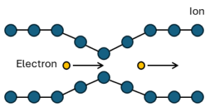
The attraction of the electron on the ion lattice will distort the lattice, moving the ions slighly towards the electron, increasing the positive charge density of the lattice in that vicinity. This positive charge density, can attract other electrons. At long distances, this attraction between electrons due to the displaced ions can overcome the electron’s repulsion and cause them to pair up. The energy that holds them together is quite weak, (order of 10-3 eV) and thermal energy can easily break the pairs. Also, the distance between electrons does not have to be close. Because the interaction is long range, paired electrons may still be 100 nm apart. This distance is usually greater than the average inter-electron distance, so many Cooper pairs can occupy the same space.
This explains how some of these special materials work, as they have layered structures. It is these layers where the electron can be transported in the crystal, because it can be easily deformed [1].
1.2 T-H-I-diagram
Elimination of the superconducting state does not only occur by raising the temperature, but also by subjecting the material to a strong magnetic field. The critical magnetic field strength, Hc, above which superconductivity is destroyed, depends upon the temperature at which the material is held. In general, the lower the sample temperature, the higher the critical field Hc. One finds:
\[H_c = H_0 = \left(1-\frac{T^2}{T_c^2}\right)\]
where H0 is the critical magnetic field strength at 0 K. Ceramic superconductors usually have a smaller Hc than metallic superconductors, i.e., they are more vulnerable to lose superconductivity by a moderate magnetic field. Moreover, another limiting parameter exists, namely, the critical current, Ic, above which superconductivity disappears. All taken, an interrelationship between temperature, current, and magnetic field strength is observed: an increase in one of these parameters decreases the critical value of the remaining two. In other words, superconductivity is only present when temperature, magnetic field strength, and current remain within a “critical space” in a T-H-I-diagram.
![The limits of superconductivity are defined in a critical T-H-I-diagram. Image taken from [2].](https://florisera.com/wp-content/uploads/2025/01/THIdiagram.avif)
The fact that it breaks at certain currents and fields really limits the applications. As increasing the critical temperature to room temperature might come at the cost of any engineering application of the material. If it is about the properties of materials as such, the pure physics, these type of materials are fantastic. However, trying to do something with the material is not always working out, from an engineering perspective.
2. AC conductivity
For Direct Current (DC) through a wire, the resistance can be calculated by the length, the diameter and the resistivity of the wire, as it can be assumed that the current goes uniformly through the wire. However, in Alternating Current (AC), there is an interaction of the electric and magnetic field in the conductor, that distributes the current towards the outside of the wire.
2.1 Skin effect & Skin depth
The electric current flows at the outer rim “skin” of the conductor. This skin effect increases with frequency, so that for high frequencies, only a thin outside layer of the conductor carries all the current. The AC current density, J, drops exponentially from the outside radius:
\[J=J_Se^{-d/\delta}\]
where JS is the current density at the surface, δ is the material parameter “skin depth”, and d is the depth beneath the surface. The skin effect causes the resistance of the conductor to increase for higher frequencies, because it is reducing the effective cross-section of the conductor.
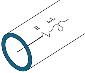
It comes from the fact that there is a current, that generates a magnetic field, which in turn creates an inductance. Recall that inductance is defined as the total magnetic flux threaded per unit current. Consequently, an AC current will prefer paths near the surface where the inductive impedance (ωL) is smaller. As the frequency increases, the current is confined more and more to the surface region. That is why for high frequency, it is better to have lots of small conductors.

2.2 Making your metal transparant
It is much more interesting when you start increasing the frequency, and how this electromagnetic wave will interact with the metal. This is a lot more interesting physics.
We know that the skin depth depends on the frequency ω. But instead of the current flowing thruogh a wire, we will study it by calculating the absorption of an electromagnetic wave that enters perpendicular into the conductor. We can use Maxwell’s equations that describe what happens when it enters a conductor. We have to translate Maxwell’s equations from a vacuum to a medium, by using the permittivity, μ, and permeability, ε, of the material. Together with Ohm’s law, the Ampere-Maxwell equation becomes:
\[\nabla^2 E = \mu\varepsilon\frac{\delta^2 E}{\delta^2 t} +\mu\sigma\frac{\delta E}{\delta t}\ ,\]
which is known as the damped wave equation. We will assume that the a plane electromagnetic wave of the form E = E0e-i(ωt-kz) is traveling in the z-direction inside this conducting material. A wave will be a solution of the damped wave equation if:
\[k^2 =\omega^2 \mu\varepsilon + i\omega\mu\sigma\]
For a good conductor and in the case that ω is not too high, the second term with σ will be dominant. In this limit and using the fact that:
\[\sqrt{i} = \pm\frac{1+i}{\sqrt{2}}\]
we get that:
\[k\approx (i\omega\mu\sigma)^{1/2}=\pm\frac{1+i}{\sqrt{2}}(\omega\mu\sigma)^{1/2}=\pm\frac{1+i}{\delta}\]
when k is imaginary, there is a loss (or attenuation). Also we defined the skin depth δ by:
\[\delta = \sqrt{\frac{2}{\omega\mu\sigma}}\]
We can observe that the skin depth decreases with increasing frequency, but also with increasing conductivity. The solution to the damped wave than becomes:
\[E = E_0 e^{-i(\omega t-z/\delta)}e^{-z/\delta}\]
This is an oscillatory wave, which amplitude declines exponentially with the skin depth defining the scale of the decline.
When a metal has high conductivity, its free electrons can move easily in response to an external electromagnetic wave (if the frequency is not too high). This movement of electrons effectively cancels out the applied electric field inside the metal. The electromagnetic radiations are thus attenuated as they penetrate in the conductor, due to the eddy currents produced in response to the oscillating electric field. This is why radio waves or microwaves cannot pass through thick metal sheets. Skin depths are of the order of centimeters at low frequencies (100 Hz), few microns at 100 MHz, and only a few nanometers for visible light (∼1014 Hz).
2.2.1 Increasing EM frequency further
Previously, we neglected the first term with ω2, which becomes more important when we keep increasing the frequency. Rather than experiencing many collisions in each cycle of the field as is the case in the low frequency regime, the elctrons will now experience many cycles of the field in-between collisions. In the low frequency regime, the electrons will reach a steady-state due to the energy loss by the collisions. In the high frequency range, this is no longer true and in this limit, the electrons will start to behave like electrons in free space.
As it is hardly scattering, the electron can accelerate and accelerate without any collision. Similarly to how the Drude model was calculated, we can assume that between collisions, Newtonian mechanics will apply, and an oscillating electric field E, given by E0e-iωt will give the electrons an acceleration:
\[m\frac{dv}{dt}=eE_0e^-{i\omega t}\]
integrating this acceleration to get the drift velocity yeilds an oscillatory drift velocity of:
\[v_D=\frac{eE_0}{i\omega m}e^{-i\omega t}\]
and the current density J = – eNevD becomes:
\[J=\frac{-N_e e^2 E_0}{i\omega m}e^{-i\omega t}\]
For high frequency regime (ωt >> 1), the AC conductivity σac = J/E then reads:
\[\sigma_{ac} = \frac{J}{E}= \frac{-N_e e^2}{i\omega m}=\frac{i\sigma_{dc}}{\omega\tau}\ ,\]
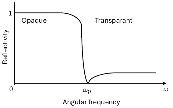
where σdc is from the classical explanation of conductivity in the drude model. J/E is imaginary, meaning that J and E are π/2 out of phase. In a normal resistor, the current and voltage are in phase and it absorps energy, but in this case it starts to behave more like a capacitance or inductance, where you store the energy. Similar to this system, at high frequency it won’t absorp energy anymore. and the metal will become transparant. The solution to the Ampere-Maxwell equation is than given by:
\[k^2=\omega^2\mu\varepsilon + i\omega\mu\sigma_{ac} = \omega^2\mu_\varepsilon – \frac{N_ee^2\mu}{m}\]
This equation can be rewritten to the form of:
\[k^2 =\omega^2\mu\varepsilon\left(1-\frac{\omega^2_p}{\omega^2}\right)\]
where ωp is the plasma frequency:
\[\omega_p=\sqrt{\frac{N_ee^2}{m\varepsilon}}\]
We can conclude that k is real (i.e. k2 is positive), when ω > ωp. In this case there is no attenuation of the amplitude of the oscillating electric field, the conductor becomes transparant. For several metals like Al, Mg, Li, etc. this plasma frequency is in the order of 1016 Hz, far above the frequency of visible light.
41.35
References
[1] Rohlf, James William, Modern Physics from A to Z, Wiley 1994.
[2] ummel, R.E. (2011). Electrical Conduction in Metals and Alloys. In: Electronic Properties of Materials. Springer, New York, NY. https://doi.org/10.1007/978-1-4419-8164-6_7
Florius
Hi, welcome to my website. I am writing about my previous studies, work & research related topics and other interests. I hope you enjoy reading it and that you learned something new.
More Posts