
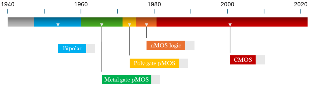
Before Metal-Oxide Semiconductor (MOS) transistors, bipolar junction transistors (BJTs) dominated due to their high speed and reliability, but they consumed a lot of power and had low input impedance. Early MOS transistors were difficult to manufacture due to surface control issues, leading to the development of pMOS with aluminum gates. pMOS was initially preferred because nMOS had a negative threshold voltage (Vt) and was unreliable. The transition to poly-silicon (poly-Si) gates improved process stability, allowed self-aligned source/drain, and enabled multi-level interconnections. nMOS became dominant due to higher electron mobility but required improvements like better oxide/interface control, poly-Si (n+) gates, and ion implantation for Vt control. LOCOS isolation and depletion load devices improved NMOS density and operation, making it the main technology for VLSI until the early 1980s. However, NMOS had high static power consumption, leading to the adoption of CMOS (Complementary MOS), which combined NMOS and PMOS for better efficiency and lower power use.
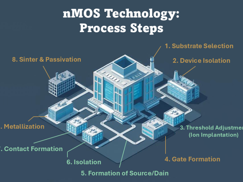
This is part of a series where I will explain the process steps of different technologies of integrated systems. This chapter is focused on the nMOS processes. Here you find links to the articles on the following topics:
Basic Process Steps (n)MOS
Substrate Selection
This slide covers the key factors in selecting a silicon substrate for NMOS or PMOS fabrication. The substrate type (N or P) determines the device polarity, while resistivity depends on the doping level, with substrate doping around 1015 cm-3 and well doping between 1016 and 1017 cm-3. The crystal orientation, typically (100) Si, affects transistor performance. Wafer size, currently 300mm, is driven by economic scaling, with future trends toward 450mm. Contamination control is crucial, as even extremely low doping levels can significantly impact electrical properties. The intrinsic carrier concentration of silicon at 300K is about 1.01 × 1010 cm-3, and doping levels as low as 0.1 ppm can influence conductivity. Surface contamination, even at atomic levels, is electrically measurable and affects device performance.
Device Isolation
Once the silicon substrate is selected, different transistors need to be electrically isolated so they don’t interfere with each other. This isolation ensures that there is no unintended current flow between the source and drain of different transistors. There are two main isolation requirements:
- Lateral isolation prevents the formation of unwanted channels between adjacent transistors. This is achieved by ensuring the depletion zones of nearby source/drain regions do not touch, which can be controlled by adjusting doping levels.
- Vertical isolation prevents poly-silicon interconnects from affecting the silicon substrate by using a SiO₂ insulating layer (field oxide).
To define the active regions (where transistors will be built), there are two main approaches:
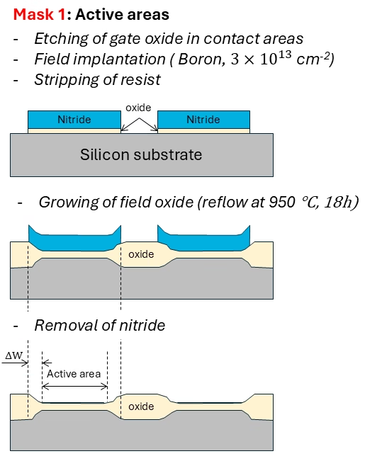
Using Two Masks (Older Method). First, a mask (M1) is used to implant dopants into selected regions. Then, a second mask (M2) is used to define oxidation areas, but misalignment issues can lead to wasted space. The other approach is using a technique called LOCOS (Local Oxidation of Silicon)
Local Oxidation of Silicon (LOCOS) is a traditional isolation technique. First, a thin pad oxide layer is grown, followed by a silicon nitride layer, which acts as an oxygen barrier. Photolithography and etching define the nitride mask, marking active areas. Thermal oxidation then grows a thick field oxide for isolation. Finally, the nitride is removed.
The main drawback is the bird’s beak effect, which reduces the active area, as shown in Figure X (note that ΔW reduces with better techniques and processes). However, LOCOS is valued for its simple process flow and high-quality thermally grown oxide.
One concern of the LOCOS (Local Oxidation of Silicon) process is the white ribbon effect, also known as the Kooi effect. In this situation, a thermal oxynitride forms at the surface of the silicon under the edges of the nitride pad. The white ribbon effect is caused by the reaction of Si₃N₄ (silicon nitride) with the high-temperature wet ambient, leading to the formation of NH₃ (ammonia). This ammonia diffuses to the Si/SiO₂ interface, where it dissociates.
When the effect is severe, the surface texture caused by these nitrides can be observed as a white ribbon around the edges of the active area. This defect leads to a reduced breakdown voltage in subsequent thermal oxides (such as gate oxides) in the active region.
Threshold Adjustment (Ion Implantation)
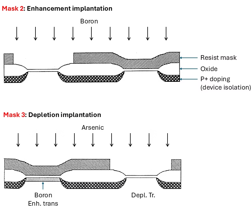
In early NMOS technology, special direct contact structures were needed since CMOS did not yet exist. Fabrication required two types of devices: enhancement and depletion mode, each needing different channel doping. Enhancement-mode NMOS (Vt > 0) required a light boron implant to adjust the threshold voltage, while depletion-mode NMOS (Vt < 0) needed an additional arsenic implant to create a built-in channel, making the transistor normally on.
To create the two types, two additional masks are required as is shown in Figure X
Gate Formation
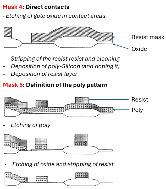
Direct contacts and polysilicon were used due to the limitations of the technology at the time, before more advanced methods like self-aligned silicides or metal gates were developed. Polysilicon was chosen because it could be easily deposited using CVD (Chemical Vapor Deposition) and could serve both as the gate material and a means of forming contacts. In the figure below, I show the different steps and the various masks required to deposit the gate.
Formation of Source/Drain (S/D)
This step involves doping the source and drain regions, as well as doping the polysilicon gate, to ensure proper conductivity and functionality of the transistor.
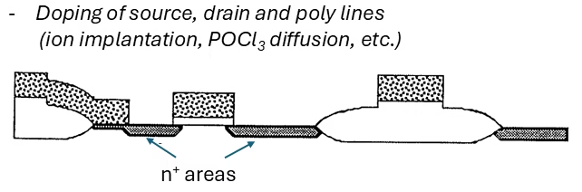
Phosphorus oxychloride (POCl₃) can be used to introduce phosphorus into the source and drain regions, creating an n-type region in the silicon, Alternatively, ion implantation can be used to directly implant dopants (such as phosphorus or arsenic) into the silicon wafer in a more controlled and precise manner. This technique allows for better control over the depth and concentration of the dopant.
Furthermore, in this process step, no mask is required, because the gate itself serves as a mask during the source and drain implantation process. The gate oxide underneath the gate provides an area where dopants cannot penetrate, ensuring that the doping is confined to the regions adjacent to the gate, which become the source and drain regions. At the same time, the poly-silicon gate also gets doped, making it more conductive.
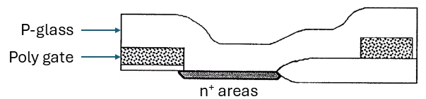
Isolation
The isolation step in NMOS fabrication is crucial for ensuring proper electrical insulation between different components and for smoothing out surface topography before metal deposition.
A 1 μm layer of phosphosilicate glass (PSG) or boron-phosphosilicate glass (BPSG) is deposited using Chemical Vapor Deposition (CVD) at around 400°C. After that, the wafer is heated to 950°C in a wet oxygen environment for about 10 minutes to reflow the P-doped glass. This is done to smoothen out the edges, improving the uniformity of metal deposition in later steps.
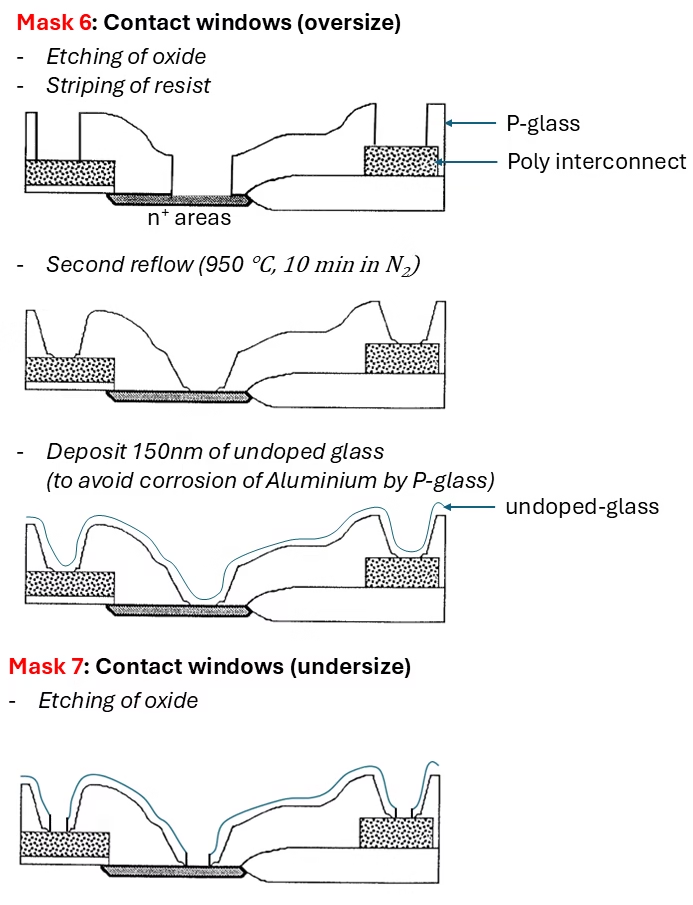
Contact Formation
In this step, contact windows are created in the insulating layers to allow connections to the underlying source, drain, and gate regions. First, an oversized contact mask is used to etch large openings. This compensates for possible misalignment errors during lithography and ensures the contact areas are properly exposed. However, aluminum cannot be deposited directly onto the phosphorus-doped glass (P-glass) because phosphorus can absorb moisture, leading to corrosion. To address this, a second reflow process is performed—following the first reflow used during isolation—to further smooth the contact walls, improving step coverage. After reflow, a thin layer of undoped silicon dioxide (SiO₂) is deposited over the P-glass to act as a barrier against corrosion. Finally, a second etch is performed using an undersized mask, which selectively removes the undoped glass in the precise locations where metal contact is needed. This final etch refines the contact shape and ensures a clean, well-defined connection before aluminum deposition.
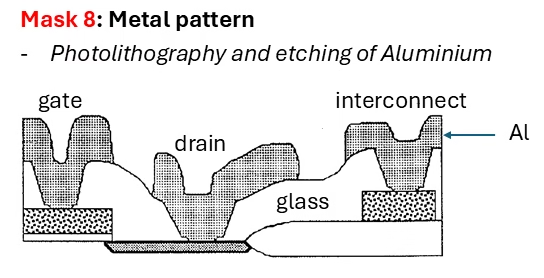
Metallization
In the metallization step, aluminum with 1% silicon (Al/1%Si) is first deposited over the wafer. Pure aluminum can diffuse into the silicon substrate at high temperatures, forming spikes that penetrate the source/drain junctions, causing electrical shorts. By adding 1% silicon, the aluminum is already saturated with silicon, reducing the tendency for additional silicon diffusion and preventing these spikes.
Etching removes excess aluminum, leaving behind only the desired metal lines that connect the source, drain, and gate regions. If aluminum were left unetched, it would create unwanted electrical connections between different components.
Sinter & Passivation
Sintering (typically at temperatures between 430–450°C for about 30 minutes in a forming gas mixture, which is 10% H₂ and 90% N₂) improves the metal-silicon contact quality by reducing the contact resistance at metal-semiconductor junctions. Additionally, the hydrogen in the forming gas helps to passivate dangling bonds at the Si-SiO₂ interface, reducing interface trap states and improving the overall transistor performance.
Finally, in the passivation step, a thin layer of SiO₂ (silicon dioxide) or sometimes Si₃N₄ (silicon nitride) is deposited over the entire wafer. This passivation layer protects the devices from moisture, dust, and mechanical stress, and also prevents metal corrosion. It significantly contributes to the long-term reliability of the chip by providing a protective barrier against environmental factors.
References
[1] R. S. Muller, T.I. Kamins, and M. Chan, “Device Electronics for Integrated Circuits“, 3rd ed., Hoboken, NJ, John Wiley & Sons, 2003.
[2] J. D. Plummer, M.D. Deal, and P.B. Griffin, “Silicon VLSI Technology“, Upper Saddle River, NJ, Prentice Hall, 2000.
[3] S. Wolf, “Microchip Manufacturing“, Lattice Press (www.latticepress.com), 2004
Florius
Hi, welcome to my website. I am writing about my previous studies, work & research related topics and other interests. I hope you enjoy reading it and that you learned something new.
More Posts