Introduction
When talking about microelectronic packaging, it refers to the protection, powering, cooling, and interconnection of integrated circuits, encompassing both the packaging of individual components and the means of electrically and thermally connecting them within a system. Each component may itself consist of several sub-components.
Table of Contents
In the past, packaging was just an afterthought, and because of that, there were many parasitic problems, thermal problems and EMC problems. Right now, its a highly multi-disciplinary branch. You’ll have to select the best suited interconnection technology for a given application and design the system as function of the possibilities and limitations of this technology. This does require a balance between cost, performance and reliability. Due to tha fact that the complexity increases faster than the feature size reduction, there is an increase of chip surface area of ~20% per year. And as the IC complexity goes up, the pin count increases. The empirical relation between number of connections on a chip and the
Traditional IC Packaging
The traditional packaging process begins with wafer thinning and dicing. Once individual dies are separated, they can be connected to the external environment using methods such as wire bonding. In the final section, I will explore various techniques used to protect the die from mechanical and environmental stress, and introduce established packaging formats like DIL, SOP, QFN, and more.
Wafer thinning
Wafer thinning is performed to prepare the wafer for packaging, typically by removing silicon from the wafer backside using coarse and fine grinding steps. The final silicon thickness is usually around 300 microns for standard packages, but it can be reduced to as little as 30 microns, depending on the application. However, back grinding induces damage to the silicon backside, which can result in electrical failures, chip cracking, and increased wafer stress and bowing. To ensure reliability, the damaged silicon layer must be removed. Several stress relief methods are illustrated in Figure 1.

Wafer dicing
After thinning, the wafer is diced into individual dies. This is a delicate process, as it involves a dicing blade cutting through the wafer. Due to the nature of the method, some degree of chipping and cracking is inherent to dicing. Distilled water is used during the process to cool the blade and to remove silicon particulates generated during cutting.
When the wafer contains low-k dielectric materials, which are brittle and porous, extra care is needed. The same applies to wafers with copper interconnects. For such cases, a two-step dicing process is used: first, a large blade is used to make shallow, gentle cuts; then, a smaller blade follows with more force, cutting completely through the wafer and even into the supporting tape underneath.

There is also a non-mechanical method known as laser dicing. However, this technique has its own challenges, as shown in Figure 3. When long laser pulses are used, significant heat is introduced into the material, which can cause damage to the silicon die and lead to redeposition of molten silicon particles along the cut edges. To reduce the heat-affected zone, short laser pulses with longer intervals between them can be applied, minimizing thermal damage and improving cut quality.

Wire bonding
To connect the I/Os of the die to the external package, one common method is wire bonding, where a thin metallic wire (typically gold or aluminum) connects a bond pad on the die to a corresponding pad on the package. One of the main advantages of wire bonding is that it does not require additional processing steps on the chip itself and can be performed directly on the die.
However, since the wire must arc upward and outward to reach the package, it requires more space, limiting packaging density. The longer wire length also increases parasitic inductance, which can affect high-frequency performance. Additionally, because wire bonds are mechanical connections, verifying electrical continuity is challenging, and if a fault is detected, repair is often difficult or impractical.
Ball bonding
There are two main wire bonding techniques. The first is ball bonding, as shown in Figure 4. In this method, the bonding tool (capillary) is heated, and the substrate is typically maintained at 150–170 °C. A small molten ball is formed at the tip of the wire. This ball is then pressed onto the die pad to form the first bond (ball bond).
After this, the capillary moves to the second bonding location—usually on the package substrate—and presses the wire down to form a wedge bond using ultrasonic energy and pressure. The wire is then clamped and broken off, completing the connection.
Ball bonding has several advantages: it supports omnidirectional pad layouts, offers high fatigue resistance, and is well-suited for high-volume production. However, bond surface cleanliness is critical for high yield and bond reliability. This can be further improved by applying a thin gold layer on any organic substrates, which enhances bondability and reduces contamination-related issues.

Wedge bonding
The other technique is wedge bonding, which uses a tool called a sonotrode to apply ultrasonic vibrations that form the bonds, as illustrated in Figure 5. In this method, both the first and second bonds are wedge-shaped. Because the wire exits the bonding tool at a fixed angle, wedge bonding is inherently unidirectional, requiring specific wire orientations during layout.
The key difference from ball bonding is that wedge bonding does not require heating the substrate. This makes it the preferred choice for applications with temperature-sensitive materials, such as bendable substrates, organic laminates, or flexible circuits.
Another major advantage is its low profile—since wedge bonding lacks the vertical loop created in ball bonding, it’s better suited for compact or low-clearance packages. Additionally, the ultrasonic energy used during bonding helps to clean the pad surface, reducing the need for perfect cleanliness and improving overall yield.
However, wedge bonding requires more horizontal space due to the wire feed angle and tool geometry. It also tends to be slower than ball bonding because it’s typically performed at room temperature and requires precise positioning (still, both techniques are slow compared to parallel interconnect methods, as they are sequential processes).

Flip chip technology
Lastly, we have the “Flip-Chip” technique, which is exactly as it implies, we mount the chip upside-down on a substrate with direct electrical connections between the chip and the substrate. It is very parallel, very fast and takes the least amount of space. Another advantage is that it creates a sealed cavity, which is required for certain applications (think of MEMS packaging). However. it does require a lot of prepatory (such as solder balls) and post-processing steps. The bad part is that if there is any misalignment, or missing contact, the chip with not work and impossible to repair. The electrical connection can be made through solder reflow joining, thermocompression (not discussed here), and adhesive bonding.
Solder Reflow Joining
Solder reflow joining is a bonding process that relies on the formation of intermetallic compounds (e.g., 95% Pb / 5% Sn) during the melting of the solder. The electrical connection is established through a conductive “bump” formed between the pads, as shown in Figure 6. There are several methods to create these solder balls, including pick-and-place, evaporation, electrolytic plating (resulting in “mushroom”-shaped bumps), and stud bumping.
In all cases, the top of the bump includes an under-bump metallurgy (UBM) layer, typically made of tungsten, to prevent solder from diffusing into the silicon. At the bottom of the bump, where it contacts the attachment pad, the copper is partially consumed by the tin, forming an intermetallic compound (IMC). This interface has slightly different thermal properties compared to the bulk materials.
The primary reliability concern is solder fatigue caused by the mismatch in thermal expansion between the chip and the substrate. As the chip heats up during operation, it expands more than the solder bumps, inducing stress. Over time, this thermal mismatch can lead to fatigue failure in the solder joints. To mitigate this, a non-conductive polymer adhesive—called underfill—is injected beneath the chip. It spreads due to capillary action and helps distribute mechanical stress, improving reliability.

Adhesive bonding
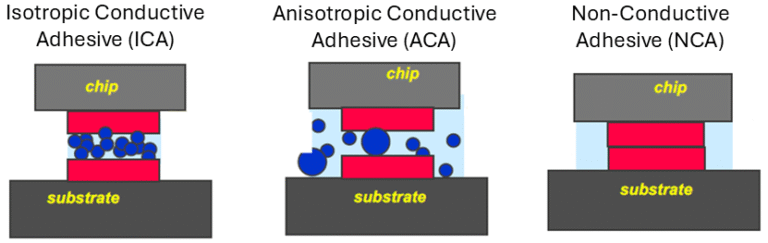
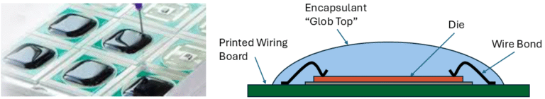
With adhesive bonding, glue is used as an underfill to hold the chip and substrate together. However, due to the nature of this bonding method, the electrical contacts typically have lower conductivity, making it unsuitable for high-speed or high-power applications. The following three options are displayed in Figure 7.
One approach is isotropic conductive adhesive (ICA), where conductive particles are mixed into the adhesive and applied sequentially to each pad. This process is relatively slow and may still require additional underfill, as the adhesive is only present on the contact points.
Another method is anisotropic conductive adhesive (ACA), which involves dispensing a polymer adhesive loaded with small conductive particles over the entire substrate surface, similar to underfill, before performing flip-chip assembly. The conductive particles align vertically under pressure, allowing current to pass only in the z-direction. However, this type of contact supports only low currents. A typical application is in smartcards.
A third option is non-conductive adhesive (NCA), where a polymer adhesive is used without conductive particles. During bonding, the pressure brings the chip’s bond pads and the substrate pads into direct contact. This method can potentially offer the highest current-carrying capacity of the three, but it requires precise process control. The bond pads must be carefully flattened and spaced evenly, which may involve mechanical milling to achieve uniform height.

Protection after bonding
After the chip has been bonded (or flip-chip assembled) onto the substrate or interposer, it requires additional protection to ensure mechanical stability, environmental resistance, and long-term reliability.
Glob-Top (Chip-on-Board)
As shown in Figure 8, Glob-Top encapsulation, is a technique where a type of liquid is dispensed on the die, so that it completely covers everything, including the wire bonds. This is a cheap and easy solution, but it does have some possible issues. Air bubbles can form, due to bad penetration of the liquid (especially near the wires). It can even damage bond wires if not done carefully. And lastly, it has to be dispensed carefully, so that the encapsulant doesnt migrate to areas you do not want them. Sometimes, a “dam & fill” technique is applied, where a small dam is created around the chip, which is than filled with a low viscosity encapsulant. These kind of technologies are being used in for example smart cards.

Transfer Molding (Plastic Packages)
ransfer molding is a common process used in semiconductor packaging, especially for plastic encapsulation of integrated circuits (ICs). It is widely used for leadframe-based packages such as DIP, QFP, SOIC, and many more. Transfer molding involves forcing a thermosetting plastic compound (typically epoxy-based) into a mold cavity where it surrounds the semiconductor die, bonding wires, and part of the leadframe, then hardens into a solid protective package. Some examples can be seen in the next section.
Established packaging
Single-chip packaging can be achieved in a wide variety of ways, with numerous methods developed over time. Even the older packaging methods are still widely used, particularly in the automotive industry, due to its low cost and high reliability. Figure 9 presents a timeline and brief overview of several packaging methods.

Lead Frame Based Packages
For lead-frame-based packaging—including DIL, SOIC, PLCC, QFP, and QFN—the chip is mounted onto a metal frame (commonly called a “spider”) and encapsulated in plastic using transfer molding. The Quad Flat No-Lead (QFN) package is a more recent development. As shown in Figure 10, only the top side of the lead frame is overmolded with resin, while the bottom side forms a land grid array, enabling direct solder attachment to the PCB. A key advantage of the QFN package is the exposed die paddle at the center of the bottom side, which can be used as a heatsink to improve thermal performance.

The number of pins (or external connections) on a chip is related to the number of circuits it contains, following an empirical relationship known as Rent’s Rule. As chip complexity increased, placing leads on just two or even all four sides of the package became insufficient. To accommodate more connections in a limited area, grid array packaging was developed.
Grid Array packaging
In grid array packaging, the chip is mounted (flip-chipped) on a laminate or ceramic interconnect substrate, which redistributes the I/O connections to an array of solder balls. The original concept, introduced by Motorola, was known as “OMPAC.” As discussed in a previous section, these solder balls enable electrical and mechanical connection through a solder reflow process. This technique is exemplified by Ball Grid Array (BGA) packages, as shown in Figure 11 (left).
To further reduce package size and thickness, BGA technology has rapidly evolved toward finer ball pitches, leading to the development of Chip-Scale Packages (CSPs). CSPs are typically no more than 20% larger than the chip itself and can feature ball pitches as small as 0.5 mm. An example is shown in Figure 11 (right).

References
Florius
Hi, welcome to my website. I am writing about my previous studies, work & research related topics and other interests. I hope you enjoy reading it and that you learned something new.
More PostsYou may also like


