

In our previous articles, we explored how NMOS and later CMOS transistors are fabricated—from the initial wafer to the final multilayer device—highlighting the key techniques used throughout the process. We also introduced the concept of transistor scaling, particularly through Dennard scaling, and noted that reducing device dimensions is not without consequences. For many years, CMOS transistors were successfully scaled using the same principles, until a critical point was reached: the minimum gate length approached 1 μm. In a later post, we will look at the truly smallest transistors, when it dips below <100 nm, in the nanoelectronics era.
Table of Contents
In this article, we dive deeper into the limitations of scaling down further during the microelectronic era, ranging from 1 μm down to 0.1 μm. In the first part of this period, spanning from 0.7 μm down to 0.25 μm CMOS technologies, the gate oxide thickness (tox) was aggressively reduced, while supply voltages remained relatively constant—a strategy known as quasi-constant voltage scaling. This approach led to extremely high electric fields within the devices, giving rise to reliability challenges such as hot carrier effects. In this article, I will explain some of the techniques that were introduced on top of the normal processes to handle these high electric fields.
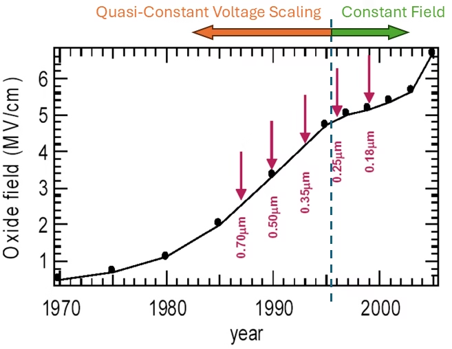
By the mid-1990s, electric fields had risen to nearly 5 MV/cm, pushing the technology to its limits. This marked a shift in the second part of the microelectronic era, from the 0.18 μm to 0.13 μm technology nodes, when voltage scaling was introduced alongside further oxide thickness reduction. This enabled what is known as constant field scaling, where the electric field remains approximately constant even as devices continue to shrink.
The figure above illustrates this transition: initially, voltage remains fixed while electric fields intensify, until a turning point is reached (the year ~1995) and voltage scaling is adopted to preserve manageable field strengths.
Submicron scaling: Quasi-constant voltage scaling
As we discussed in the previous article, high electric fields in scaled CMOS technologies introduce several challenges, and some of the key techniques used to mitigate these effects include Anti-Punch Through (APT) implants and Lightly Doped Drain (LDD) structures, also known as spacer technology. To address punch-through specifically in PMOS transistors, p⁺ polysilicon was introduced for the gate. This improved the threshold voltage and enhanced gate control, helping to suppress punch-through..
Salicides
However, this introduced a new challenge: how to interconnect p⁺ and n⁺ polysilicon gates, since the direct contact between them forms a pn junction, which behaves like a diode—and is not something you want in CMOS logic. The solution was self-aligned silicide (salicide) technology, which enables low-resistance, self-aligned contacts on both p⁺ and n⁺ regions without creating diode junctions or requiring complex metal routing.
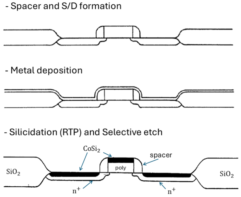
Figure 2 shows the process of forming self-aligned silicides (salicides). We start at the stage where the spacers have been formed using standard CMOS processing. A transition metal layer—commonly titanium (Ti), cobalt (Co), or nickel (Ni)—is then deposited over the wafer. These metals will later form silicides such as TiSi₂, CoSi₂, or NiSi.
The wafer undergoes a Rapid Thermal Process (RTP), which causes the metal to react with exposed silicon in the source, drain, and gate regions to form metal silicide. Since the metal does not react with silicon dioxide, no silicide forms on the spacers or isolation oxides (hence the “self-aligned”). After the RTP, any unreacted metal is selectively removed by chemical etching, leaving silicide contacts only in the active regions.
Rapid Thermal Annealing
Rapid Thermal Annealing (RTA) is a rapid thermal process that involves heating a single wafer at the time, and is one of the technological break throughs that made salicides happen. The dopants inside the wafer can be activated by a heat threatment. In other words, right after ion implantation, these dopant atoms are randomly sitting inside the crystal lattice. They need to move to the correct lattice positions (substitutional sites) to become electrically active. This is done by heating the wafer.
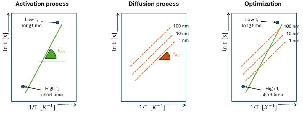
To activate the dopants, you require a certain activation energy (EA). The Arrhenius equation describes how the rate of a thermally activated proces increases very rapidly with temperature:
\[\text{Rate = }\frac{1}{t}=A\text{exp}\left(-\frac{E_{A}}{kT}\right)\]
In the Figure 3 on the left, the green line shows the relationship between temperature and time needed to achieve activation. In this case it could represent the threshold where 95% of all implanted dopants is activated, meaning that anything above the line is activated up to that threshold, and below the line not enough dopants are activated. The steepness of the curve depends on the activation energy (EA1). You can rech the needed activation in two ways. Either with at a low temperature, but for a long time. Or at a high temperature, but for a short time. Both operations could technically give you the same activation level.
However, there is another important part that we need to look at, that is diffusion. The middle figure shows lines of constant diffusion (1, 10, and 100 nm). Meaning that for a certain temperature, the longer you wait, the more it diffuses. These diffusion processes also has its own activation energy (EA2).
Lastly, on the right figure we put both together. There is an optimization needed because both processes have different EA‘s. Because of that, it is better to have high temperatures for a short time period, as this reaches the activation threshold, but minimizes dopant diffusion, keeping them where you implanted them.
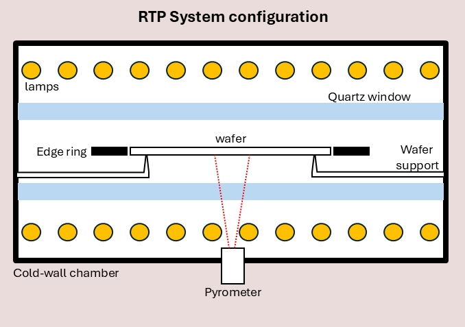
RTP Systems
These RTP-RTA systems became the standard in the mid-1980’s and were able to heat silicon wafers up to 1000 °C in just a few seconds. This was made possible by high intensity lamps or lasers. Cooling the wafer was important not to break it by the thermal shock.
LATID
Previously, we saw that a doping gradient helps to reduce the high electric fields present in a device. Techniques such as Lightly Doped Drain (LDD) and Heavily Doped Drain (HDD) were developed, which required the use of a sidewall spacer. T. Hori and K. Kurimoto introduced a new technique called Large-Tilt-angle Implanted Drain (LATID). This method implants ions at a large tilt angle, allowing them to reach underneath the gate. As a result, the sidewall spacer can be eliminated, while still maintaining self-alignment (no additional mask is required). In their paper, the authors wrote:
“The LATID achieves improved current drivability by more than 50 percent and improved hot-carrier lifetime by more than three orders of magnitude as compared with a conventional LDD. The LATID technique is most promising for applications to submicrometer ULSI under 5-V operations.”
Figure 5 shows the process sequence for LATID without sidewall spacers.
![Fig 5. Process sequence for a LATID device without sidewall spacers. Image taken from [1].](https://florisera.com/wp-content/uploads/2025/04/LATID.avif)
Aggressive Lg-scaling
With technologies above 0.25 μm, we saw strong scaling down of the gate oxide thickness, but only limited voltage scaling. This resulted in extremely high electric fields, leading to issues such as hot carrier effects, ultimately forcing a change in scaling strategy: from 0.25 μm to 0.13 μm technology, the supply voltage scaled more or less together with the gate oxide thickness (constant field scaling).
This change limited how much gate voltage could be applied above the threshold — effectively reducing the gate overdrive. Since the drive current is given by:
\[I_D \sim C_{ox}\frac{W}{L}(V_G-V_T)^2\ ,\]
a lower gate overdrive directly reduces the current. To compensate and maintain performance, engineers began aggressively scaling down the gate length L, which increases ID despite the reduced overdrive. This strategy became prominent between the 0.25 μm and 0.13 μm nodes, as shown in Figure 6, where gate lengths are actually smaller than the nominal technology node. However, this aggressive scaling also led to a significant increase in leakage current — a major challenge in modern device design. Nevertheless, effective solutions were developed to mitigate these issues, as discussed in the next section.
![Fig 6. Logic technology node and transistor gate length versus the calendar year. Image taken from [2].](https://florisera.com/wp-content/uploads/2025/04/aggressive-Lg-scaling.avif)
Front-end-of-Line (FEOL) Process Flow
During this period several improvements happened in the front end of line process flow, that help against the short channel effects. In this section I will list them up with a short explanation on how it is done.
Shallow Trench Isolation (STI)
Shallow Trench Isolation (STI) is a technique used in the modern semiconductor industry to isolate transistors on a chip. In my previous posts on NMOS and CMOS process steps, I explained LOCal Oxidation of Silicon (LOCOS), which is a similar method but causes surface issues at small scales.
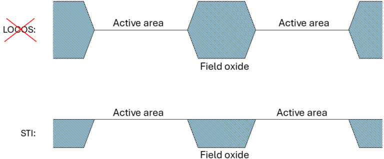
STI solves this by etching narrow and shallow trenches into the silicon substrate, which are then filled with silicon oxide, as shown in Figure 7. This newer technique required the development of another process called Chemical Mechanical Polishing (CMP), which is used to flatten the surface.
The exact method for creating STI with CMD deserves an article on its own, as it involves careful tuning — especially of the polish rate. Over-polishing or incomplete polishing can be highly detrimental to transistor performance.
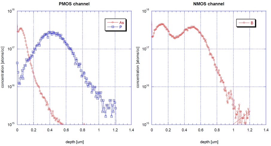
Channel doping
During the process of defining n-type and p-type wells for NMOS and PMOS transistors, multiple lithography and ion implantation steps are used. Previously, a single ion implant was sufficient, but at this stage, two implants are introduced.
The first is a high-energy well implant, which penetrates deep enough to reach beneath the field oxide and defines the n-well and p-well regions. The second is a low-energy implant, used for threshold voltage adjustment and leakage current suppression.
For PMOS transistors, phosphorus is used for the high-energy well implant, and arsenic for the low-energy adjustment. For NMOS transistors, two boron implants with different energies are used.
Figure 8 shows the resulting doping concentration profile in the channel region as a function of depth.
HALO implant
During CMOS scaling down to the 1 μm node, extension implants (also known as Lightly Doped Drain or LDD implants) were introduced to reduce electric field peaks at the drain junction. However, they extend the source/drain region further into the channel, effectively shortening the channel length and worsening short-channel effects (SCE). As a result, the threshold voltage, VT, starts to roll off and leakage increases.
Ideally, we want VT to remain independent of the channel length. To address this, HALO implants (also known as pocket implants) were introduced. A HALO implant locally increases the doping concentration around the tip of the extension region, just under the gate edge and before the spacer. It uses the same dopant type as the channel but is implanted at an angle to reach underneath the gate. This localized doping helps suppress SCEs and prevents VT from rolling off too early.
![Fig 9. Schematic representation of an NMOS transistor in short and long channel dimensions. Core transistors are fabricated by using LDD extensions, an antipunchthrough implantation and HALOS. By decreasing the channel length, the HALOS overlap, increasing the overall channel doping. Image is taken from [3].](https://florisera.com/wp-content/uploads/2025/04/HALO_v2.avif)
As shown in Figure 9, HALOs were implemented along with the anti-punchthrough layer to further mitigate SCEs. However, they introduce non-uniform channel doping, especially in short-channel devices. In these cases, the halo from the drain side can overlap with the one from the source, increasing the doping concentration in the center of the channel. This raises the threshold voltage of very short transistors — a phenomenon known as the Reverse Short-Channel Effect (RSCE), which is common in aggressively scaled CMOS technologies with high halo doping.
As you can imagine, this limits the gate overdrive, which in turn reduces drive current and can also impact performance.
Back-end-of-Line (BEOL) Process Evolutions
When looking beyond the transistors, as everything scales down, so do the connections to the transistors. With a smaller gate length, gate delay decreases due to reduced channel length and capacitance. However, for interconnects, scaling has the opposite effect. As interconnects become narrower, their resistance R increases. At the same time, reduced spacing between lines increases the capacitance C. As a result, the interconnect delay t = RC increases. One way to mitigate this problem is by using a metal with lower resistivity ρ, such as copper, instead of aluminum.
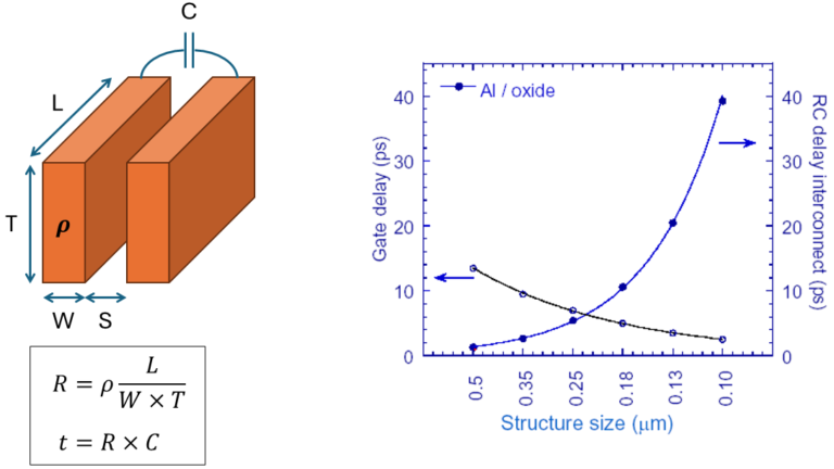
Copper has a lower resistivity than aluminum, so for interconnects with the same dimensions, it results in lower resistance. It also offers better resistance to electromigration. However, there are many downsides as well. It creates deep trap levels in silicon, and its ions diffuse rapidly through dielectrics and silicon, even at low temperatures. Additionally, it forms harmful silicates and oxidizes easily. Incorporating copper into transistor fabrication requires major process changes, including stricter contamination control and continuous monitoring. Wherever copper is used, diffusion barriers and corrosion control are essential.
Despite these challenges, copper was successfully integrated into semiconductor processes using a method called Damascene. This technique draws its name from the ancient art of inlaying gold into non-precious metals, originating in Damascus, Syria.
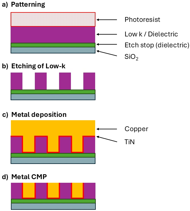
The Damascene process is an additive method and avoids the need to etch copper directly. Figure 11 shows the different steps for this process. First, photoresist is patterned using a mask. Then, the low-k dielectric is etched to form the trenches and vias where interconnects are needed. Next, a diffusion barrier is deposited to prevent copper from contaminating the surrounding material. Afterward, a copper seed layer is added using PVD, followed by electroplating to fill the structures with copper (these two steps are not shown independently here). Finally, chemical mechanical polishing is used to planarize the surface, leaving copper only in the desired region
References
[1] T. Hori and K. Kurimoto, A new MOSFET with large-tilt-angle implanted drain (LATID) structure, IEEE Electron Device Letters, vol 9, issue 6, 1988.
[2] M. Darwish, Memristive Behavior In Vanadium Dioxide Elements: Simulation And Modeling, Presented at Tavaszi Szél – Spring Wind 2019, Debrecen (Hungary).
[3] S. Bonaldo, et al., Influence of Bulk Doping and Halos on the TID Response of I/O and Core 150 nm nMOSFETs, Electronics, 12(3), 543, (2023).
[4] J. D. Plummer, M. D. Deal and P. B. Griffin, “Silicon VLSI Technology: Fundamentals, Practice and Modeling,” Prentence Hall Electronics and VLSI Series, 1999
Florius
Hi, welcome to my website. I am writing about my previous studies, work & research related topics and other interests. I hope you enjoy reading it and that you learned something new.
More Posts