RSS Daily tech news
  • You’ve never seen atoms like this before: A hidden motion revealed
    A pioneering team at the University of Maryland has captured the first-ever images of atomic thermal vibrations, unlocking an unseen world of motion within two-dimensional materials. Their innovative electron ptychography technique revealed elusive “moiré phasons,” a long-theorized phenomenon that governs heat, electronic behavior, and structural order at the atomic level. This discovery not only confirms […]
  • This Algorithm Just Solved One of Physics’ Most Infamous Problems
    Using an advanced Monte Carlo method, Caltech researchers found a way to tame the infinite complexity of Feynman diagrams and solve the long-standing polaron problem, unlocking deeper understanding of electron flow in tricky materials.
  • A simple twist unlocks never-before-seen quantum behavior
    Scientists have discovered a revolutionary new method for creating quantum states by twisting materials at the M-point, revealing exotic phenomena previously out of reach. This new direction dramatically expands the moiré toolkit and may soon lead to the experimental realization of long-sought quantum spin liquids.
  • Scientists just recreated a 1938 experiment that could rewrite fusion history
    A groundbreaking collaboration between Los Alamos scientists and Duke University has resurrected a nearly forgotten 1938 experiment that may have quietly sparked the age of fusion energy. Arthur Ruhlig, a little-known physicist, first observed signs of deuterium-tritium (DT) fusion nearly a decade before its significance became clear in nuclear science. The modern team not only […]
  • This breakthrough turns old tech into pure gold — No mercury, no cyanide, just light and salt
    At Flinders University, scientists have cracked a cleaner and greener way to extract gold—not just from ore, but also from our mounting piles of e-waste. By using a compound normally found in pool disinfectants and a novel polymer that can be reused, the method avoids toxic chemicals like mercury and cyanide. It even works on […]
  • Self-lighting chip uses quantum tunneling to spot a trillionth of a gram
    Imagine detecting a single trillionth of a gram of a molecule—like an amino acid—using just electricity and a chip smaller than your fingernail. That’s the power of a new quantum-enabled biosensor developed at EPFL. Ditching bulky lasers, it taps into the strange world of quantum tunneling, where electrons sneak through barriers and release light in […]

Tunneling effect at semiconductor/oxide interfaces

by Florius
Abstract image of a blue glowing tunnel with a central sphere emitting electric-like tendrils, representing a stylized quantum or energy field.

1. Step potential: E > V

Electron tunneling is a phenomenon commonly observed at semiconductor/insulator or metal/insulator interfaces, particularly when the insulating layer is thin, typically a few nanometers thick. To grasp its intricacies, let’s simplify the scenario.

We begin by considering a 1D barrier problem for a stream of particles. The current density (J), relating to the particle density, can be expressed as:

\[\frac{\partial\rho}{\partial t}+\nabla\cdot\textbf{J} = 0\ ,\]

where ρ denotes the particle density. If we conceive ψ as the particle beam, then |ψ|2 also represents the particle density, thus linked to the current J.

When examining a semiconductor/insulator/semiconductor interface, we can model it with a rectangular potential comprising three regions, as is shown in Figure 1. Regions 1 and 3 exhibit zero potential, while region 2, ranging from (-a; a), features a finite potential V. Here, V remains constant but nonzero.

Quantum mechanical diagram with wavefunctions ψ1,ψ2,ψ3ψ1​,ψ2​,ψ3​ across three regions. A finite rectangular potential barrier of height VV and width 2a2a separates regions. Arrows represent incident, reflected, and transmitted wave components, with exponential terms showing wave propagation.
Fig 1. Quantum tunneling through a finite potential barrier where the particle energy E>VE>V: Transmission and partial reflection illustrated across three regions.

In classical terms, imagine kicking a football with sufficient kinetic energy—it flies over the barrier. Similarly, in quantum physics, when the energy E vastly exceeds V as is shown in Figure 1, the transmission coefficient nears 1, indicating seamless passage across the boundary. However, as E approaches V, this smooth transition is no longer true. When they align, the transmission coefficient oscillates between 0 and 1. Notably, only when the barrier width (2a) precisely matches an integral number of half wavelengths, does the barrier become transparent to incoming electrons. In the following section, we delve deeper, exploring the scenario when energy falls below the barrier, necessitating tunneling through it.

2. Step potential: E < V

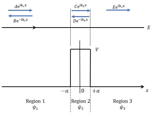
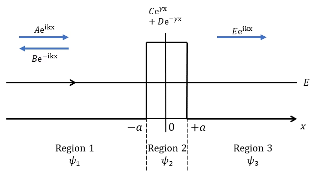
Continuing from the preceding section, we now examine scenarios where the energy level dips below the potential threshold, illustrated in Figure 2. In classical terms, this situation is similar to tossing a ball, only to have it fall short of clearing the obstacle and rebounding back. But this classical analogy no longer holds at the quantum level.

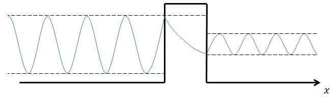
Similar to earlier, regions 1 and 3 maintain their oscillating nature, governed by a combination of oscillating wavefunctions of an electron. However, in region 2 the particle beam encounters the barrier, it undergoes absorption, characterized by a mix of exponential functions. When an incoming wave with a certain energy enters region 2, its signal diminishes exponentially as it approaches zero upon reaching the boundary condition x=a. Yet, under specific conditions -such as sufficient energy or a thin barrier – the wave function doesn’t fully extinguish at x=a. Instead, there exists a probability, albeit small, for the beam to traverse the barrier, persisting with an oscillatory behavior. Figure 3 shows an illustration of how this looks like.

Within the potential barrier, a reflecting wave emerges at the boundary x=a with an amplitude D. This phenomenon, too, follows an exponential decay pattern as it succumbs to absorption. It’s worth noting that while my description may imply a temporal aspect, the solution to the problem remains time-independent.

Quantum tunneling illustration with wavefunctions ψ1,ψ2,ψ3ψ1​,ψ2​,ψ3​ across three regions. A rectangular barrier of height VV and width 2a2a lies between −a−a and +a+a. Region 2 shows decaying and growing exponential solutions Ceγx+De−γxCeγx+De−γx. The incident wave AeikxAeikx, reflected wave Be−ikxBe−ikx, and transmitted wave EeikxEeikx are indicated with blue arrows. Energy line EE lies below the barrier height.
Fig 2. Quantum tunneling through a potential barrier where the electron energy E<VE<V: Classically forbidden region with evanescent wave in Region 2.
Graph showing a quantum wavefunction encountering a rectangular potential barrier. The wave oscillates before the barrier, decays exponentially inside it, and re-emerges with smaller amplitude after the barrier. The potential step is marked with solid black lines, and energy levels are indicated with dashed horizontal lines.
Fig 3. Illustration of quantum tunneling: a wavefunction partially penetrates and decays inside a potential barrier, continuing with reduced amplitude on the other side.

The electron wave function is obtained by solving the one-dimensional (time-independent) Schrödinger equation

\[\left[ \frac{\hbar^2}{2m^*}\frac{\partial^2}{\partial x^2} + V(x)\right]\psi (x) = E\psi (x)\]

where V(x) depends on the region the electron is in.

Region 1 & 3

In these two regions, when x<-a and x>a, the potential V(x)=0.

The solution for the wavefunction, ψ, is than the following:

\[A\textrm{exp}(ikx) + B\textrm{exp}(-ikx)\]

and

\[E\textrm{exp}(ikx)\]

Region 2

Within the potential barrier (when it falls between -a and a), the potential is V(x)=V0.

The solution to the wavefunction in this region is given by:

\[C\textrm{exp}(\gamma x) + D\textrm{exp}(-\gamma x)\]

Where A is the amplitude of the incoming wave on the left side, and E is the amplitude of the outgoing wave on the right side, furthermore:

\[k=\frac{\sqrt{2m^* E}}{\hbar}\ ,\]

\[\gamma = \frac{\sqrt{2m^*(V_0-E)}}{\hbar}\]

2.1 Transmission coefficient

The transmission coefficient is then defined as the ratio between the transmitted and incident probability flux.

\[T = \frac{\textbf{j}_{trans}}{\textbf{j}_{inc}}=\frac{\mid E\mid^2}{\mid A\mid^2}\]

To solve it, we have to impose the continuit of the solution and their derivatives (denoted by the ‘ ) at the boundaries.

\[\psi_1(0) = \psi_2(0)\] and \[\psi_1^{‘} (0) = \psi_2^{‘}(0)\]

\[\psi_2(0) = \psi_3(0)\] and \[\psi_2^{‘}(0) = \psi_3^{‘}(0)\]

In the limit γa >> 1, corresponding to the weak transmission limit (electron wave length is small compared to the barrier width W):

\[T(E)\approx \left(\frac{4k\gamma}{k^2+\gamma^2}\right)^{2}e^{(-4\gamma a)}\propto e^{\left(-2W\sqrt{2m^* (V_0-E)}/\hbar\right)}\]

This relationship highlights the exponential decline of the transmission coefficient concerning both the barrier width, W, and its height, V0. Consequently, as barriers become thicker, the likelihood of tunneling diminishes exponentially, approaching zero. This behavior is illustrated in Figure 4, which charts the transmission coefficient T(E) against energy E relative to V0.

For substantial barrier thicknesses (e.g., 10nm), tunneling activity below E/V0 = 1 is extremely limited, with only a faint tail observed below this threshold. Also note that oscillations emerge around E, indicating energy levels at which electrons cannot transmit through. Conversely, smaller barriers (e.g., 2nm) exhibit quite a large transmission coefficient below E/V0 = 1, making a substantial tunneling current possible.

Graph showing quantum tunneling transmission T(E)T(E) as a function of energy EE normalized by barrier height V0V0​. A solid curve (10 nm barrier) displays sharp oscillations above E/V0=1E/V0​=1, while a dotted curve (2 nm barrier) shows a smoother transition. The y-axis represents transmission probability (0 to 1), and the x-axis is labeled E/V0E/V0​ (0 to 2).
Fig 4. Transmission probability T(E)T(E) vs. normalized energy E/V0E/V0​ for a rectangular potential barrier of two different widths: 10 nm (solid line) and 2 nm (dotted line).

3. MOSFET tunneling

in MOS (Metal-Oxide-Semiconductor) devices such as MOSFETs (Metal-Oxide-Semiconductor Field-Effect Transistors), the voltage drop across the SiO2 layer is controlled by the gate terminal voltage. By applying a specific voltage to the gate terminal with respect to the source terminal, the electric field generated across the SiO2 layer can be manipulated, affecting the tunneling behavior of electrons through the oxide layer. We can consider two different regimes for tunneling of electrons through an Si/SiO2 interface, depending on the value of the voltage drop V0x across the insulating layer.

Direct tunneling

Energy band diagram of a MOS structure with n-type silicon (n-Si) on the left, an SiO₂ barrier in the middle, and a metal contact on the right. The conduction band EcEc​, valence band EvEv​, and Fermi level EFEF​ are shown bending near the SiO₂ interface. Voltage VV, potential drop VoxVox​, and barrier height ϕbϕb​ are labeled with arrows.
Fig 5. Energy band diagram of a metal-oxide-semiconductor (MOS) structure showing the energy levels across n-type silicon (n-Si), silicon dioxide (SiO₂), and metal. Applied voltage V affects the oxide potential Vox​ and the band bending in the semiconductor. Illustrates the direct tunneling.

When the energy potential, qV0x, is less than the potential barrier, φb, at the Si/SiO2 interface (approximately 3.2 eV), electrons undergo tunneling through a trapezoidal barrier, known as direct tunneling. Using the Wentzel–Kramers–Brillouin (WKB) approximation, one can derive:

\[T_{DT}(E,V_{ox})\approx\textrm{exp}\left[-\frac{4\sqrt{2m^*}}{3e\hbar E_{ox}}\left((\phi_b-(E-E_F))^{3/2}-(\phi_b-(E-E_F)-eV_{ox})^{3/2}\right)\right]\]

Fowler-Nordheim tunneling

Energy band diagram of a MOS structure under Fowler–Nordheim tunneling conditions. The SiO₂ barrier is triangular due to a high electric field. Bands for conduction (EcEc​), Fermi level (EFEF​), and valence band (EvEv​) are shown bending near the oxide. A green electron tunnels from n-Si through the SiO₂ into the metal contact. Energy drops qVoxqVox​ and qVqV, and barrier height ϕbϕb​ are labeled.
Fig 6. Band diagram illustrating Fowler–Nordheim tunneling in a metal–oxide–semiconductor (MOS) structure. Under a high electric field, electrons tunnel through the triangular barrier formed in the SiO₂ layer from the n-type silicon into the metal.

When exceeds φb, electrons tunnel through a triangular potential barrier, a phenomenon known as Fowler-Nordheim tunneling. Within the WKB approximation, the tunneling probability is described as:

\[T_{FN}(E,V_{ox})\approx\textrm{exp}\left[-\frac{4\sqrt{2m^*}}{3e\hbar E_{ox}}(\phi_b-(E-E_F))^{3/2}\right]\]

The current density due to the tunneling of electrons at a semiconductor/oxide interface is given by:

\[J=\frac{em^*(k_BT)}{(2\pi)^2\hbar^3}\int^{\infty}_{0}T(E_x)ln\left(\frac{1+\textrm{exp}\left((E_F-E_x)/k_BT\right)}{1+\textrm{exp}\left((E_F-eV-E_x)/k_BT\right)}\right)dE_x\]

The tunneling current can be calculated (numerically) by using the expressions of the transmission coefficient (T)  corresponding to the Direct or Fowler-Nordheim tunneling regimes.

Fig 7. Fowler–Nordheim plots in the forward biasing condition. Image taken from [1].

A development of the exponential term of the Fowler-Nordheim tunneling probability for E ≈ EF fits with measured data as can be seen in Figure 7 and leads to an approximate expression for the Fowler-Nordheim tunneling current:

\[J_{FN}(V)=A\left(\frac{V_{ox}}{t_{ox}}\right)^{2}\textrm{exp}\left(\frac{-Bt_{ox}}{V_{ox}}\right)\ ,\]

where the terms A and B are:

\[A=\frac{e^3}{16\pi^{2}\hbar \phi_b}\]

\[B=\frac{4\sqrt{2m^*}}{3e\hbar}\phi^{3/2}_b\]

3.1 Advancements in nanoelectronics

Scaling down dimensions proved effective during the microelectronics era, from 1μm to 100nm. However, this required the adoption of new materials and modifications to the MOSFET structure itself to remain viable. Silicon, known for its remarkable properties, served as the cornerstone material, offering semiconductor attributes like n-type, p-type, poly-silicon, and silicides, alongside a stable SiO2 insulator. Scaling the thickness of SiO2 reached a limit due to escalating gate leakage caused by electron tunneling. The probability of electron tunneling through the SiO2 layer is represented by etox, thus, as tox decreases, undesired leakage current rises. As previously demonstrated, with W representing the insulator’s thickness.

However, the objective isn’t merely to minimize tox but to maximize Cox. To achieve this, novel materials were introduced with a relative permittivity (εHK) significantly greater than that of SiO2, denoted as “high-κ materials”. The premise is to utilize tHK >> tox. This necessitates the introduction of Equivalent Oxide Thickness (EOT) as a distinct concept from tox, enabling the creation of gates with larger oxide thicknesses while maintaining the same oxide capacitance as SiO2.

\[EOT = t_{HK}\cdot (\varepsilon_{ox}/\varepsilon_{HK})\],

where εox = 3.9. The advantage of this approach lies in its scalability, allowing for further reduction of EOT.

Fig 8. Image taken from [2].

However, the persistent challenge remained with Si oxidation, which is inherently difficult to prevent at the interface. One of the advantages of SiO2 lies in its ability to form a robust interface with thermally grown Si, providing effective surface passivation. Any deposition process results in a compromised interface with increased surface states. Hence, even with the adoption of high-κ materials, a thin layer of SiO2 is retained between the high-κ material and Si substrate. It’s essential to note that this adjustment slightly alters the capacitance (Cii / ti ).

The total capacitance is given by the formula:

\[(C_{tot})^{-1}=(C_{HK})^{-1}+(C_{SiO2})^{-1}\],

and the effective permittivity (εeff) is calculated as:

\[\varepsilon_{eff}=t_{tot}\cdot\frac{\varepsilon_{hk}\varepsilon_{SiO2}}{t_{HK}\varepsilon_{SiO2}+t_{SiO2}\varepsilon_{HK}}\].

Fig 9. Gate leakage current as a function of the equivalent oxide thickness. Image taken from [3].

4. References

[1] S. Vaziri, M. Belete, E. Dentoni Litta, A. D. Smith, G. Lupina, M. C. Lemmea and M. Östling, “Bilayer insulator tunnel barriers for graphene-based vertical hot-electron transistors”, nanoscale, vol. 30, 2015.

[2] Ralph Smeets, “Intel kondigt transistor met high-k metalen gate aan,” Tweakers, Nov. 4, 2003, [Online]. Available: https://tweakers.net/nieuws/29510/intel-kondigt-transistor-met-high-k-metalen-gate-aan.html. [Accessed: May. 11, 2024]

[3] Contact me if you know the source of this figure.

Florius

Hi, welcome to my website. I am writing about my previous studies, work & research related topics and other interests. I hope you enjoy reading it and that you learned something new.

More Posts

Leave a comment

This site uses Akismet to reduce spam. Learn how your comment data is processed.