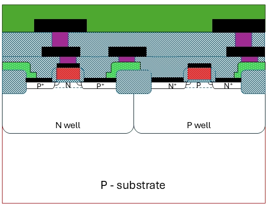

1. Doping a Semiconductor
It is possible to dope an intrinsic semiconductor in order to increase the concentration of one of the free carrier types. The semiconductor is then referred to as extrinsic. Depending on whether the doping atoms are “donors” or “acceptors“, the extrinsic semiconductor is n-type or p-type.
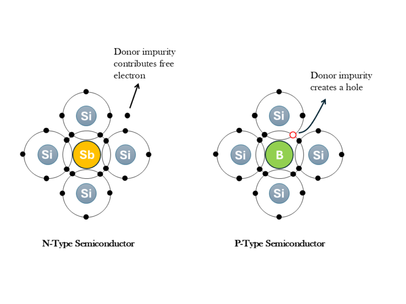
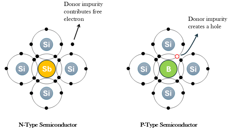
If one of the atoms of the Si crystal lattice is substituted by an atom of the Vth column of the elements (like Antimony, Arsenic or Phosphorous), this atom can satisfy the 4 covalent bonds of Si and present an extra electron. This electron is weakly bonded and can participate in the electrical conductor. We call this an n-type semiconductor.
If one of the Si atoms in the crystal lattice is substituted by an atom of the IIIrd column of the elements (like Boron), this atom can only satisfy 3 covalent bonds with its Si neighbours, lacking the electron for the last bond. This corresponds to the formation of a hole (i.e. lack of an electron) in the valence band. We call this a p-type semiconductor.
2. Energy Levels of Donors and Acceptors
A donor atom is an atom with one more valence electron than the atoms of the host lattice. The extra valence electron of the doping atom in its lowest energy state lies as an impurity level in the bandgap, close to the conduction band. Because it is close to the conduction band, only a small thermal energy2 is required for this electron to jump to the conduction band. The donor atom is then ionized and positively charged. The concentration of donor atoms is conventionally referred to as ND, and that of ionized donor atoms is ND+. At room temperature, for most semiconductors, ND+≈ ND. We will therefore use the symbol ND for the concentration of ionized donor atoms.
An acceptor atom has one valence electron less than the atoms of the host lattice, and gives rise to an electronic state located in the forbidden gap close to the valence band. An electron from the valence band only needs a small thermal energy to populate this level. This process leaves a hole in the valence band. The acceptor is then said to be ionized, and is negatively charged. The concentration of acceptor atoms is NA, that of the ionized acceptor atoms is NA–. At room temperature, NA– ≈ NA. We will therefore use NA for referring to the ionized acceptors.
The charge neutrality in the semiconductor requires that:
\[N_D + p = N_A + n\]
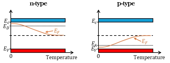
Due to the doping of the semiconductor, the Fermi level shifts closer to the conduction band for an n-type semiconductor and closer to the valence band for a p-type semiconductor. This is shown in Figure 2. We can look at two types of extrema. Firstly, increasing temperature shifts the Fermi level back toward the intrinsic Fermi level because thermal excitation generates a significant number of intrinsic electron-hole pairs, reducing the relative impact of doping. Secondly, excessive doping can shift the Fermi level inside the conduction band (for n-type) or inside the valence band (for p-type). This happens in degenerate semiconductors, where the doping concentration is so high that the material starts exhibiting metallic behavior.
Note that there is a window in which the semiconductor behaves as an extrinsic semiconductor. At very low temperatures, the donor or acceptor atoms are not ionized. As temperature increases the ionization process is complete and the carrier concentration increases to a level that is dictated by the level doping, this is the extrinsic regime. For quite a large temperature range, this concententration (and thus the conductivity) remains unchanged, until the temperature becomes too hot and the thermally generated carriers begin to dominate. The effect of dopants is lost at very high temperatures and the semiconductor essentially shows “intrinsic” behavour again.
3. Carrier Concentration at Equilibrium
The concentration of carriers is now different from an intrinsic semiconductor due to the doping we introduced into the crystal lattice. However, with the equation we obtain from the intrinsic semiconductors (n•p = ni2) and the equation of the charge neutrality from the previous section, we can calculate the carrier concentration in an extrinsic semiconductor, given the fact that it is at equilibrium.
For ND > NA, the semiconductor is n-type. The electrons then are the majority carriers and the holes are the minority carriers. The majority carrier concentration can then be expressed as:
\[n = \frac{1}{2}\left(N_D-N_A+\sqrt{(N_D-N_A)^2+4n_i^2}\right)\]
and the minority carrier concentration is:
\[p=\frac{n_i^2}{n}\]
On the other hand, when NA > ND, the semiconductor is said to be p-type. then:
\[p = \frac{1}{2}\left(N_A-N_D+\sqrt{(N_A-N_D)^2+4n_i^2}\right)\]
\[n=\frac{n_i^2}{p}\]
the holes are now the majority carriers, and the electrons the minority. In both cases, the position of the Fermi level can be found from n or p, more info here. One obtains for a semiconductor in equilibrium:
\[n=n_i\cdot e^{\frac{E_f-E_i}{kT}}\]
for the free electron concentration. Analogously, the free hole concentration in equilibrium is:
\[p=n_i\cdot e^{\frac{E_i-E_f}{kT}}\]
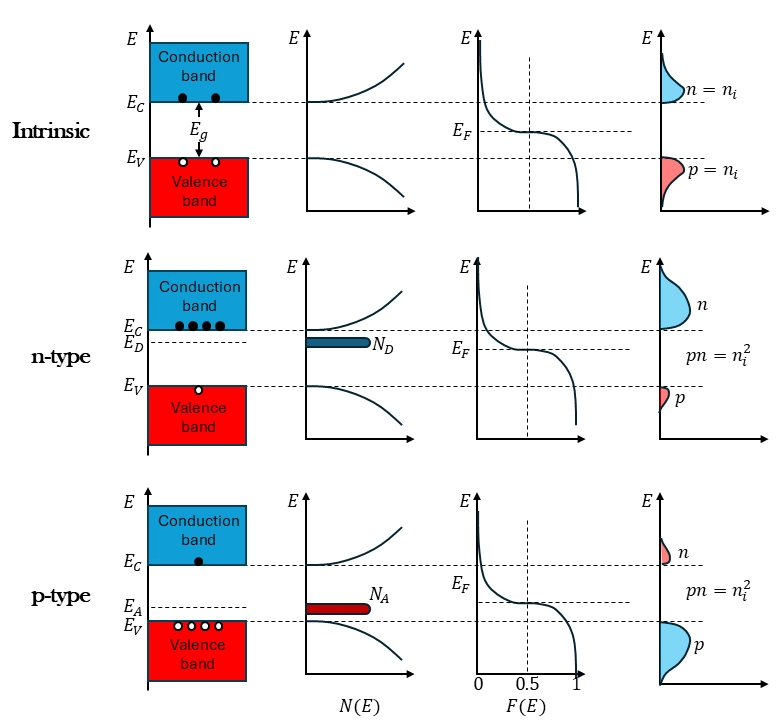
As mentioned many types before, the occupation of electron and hole states at room temperature is determined by the density of states, N(E), and the Fermi-Dirac distribution, F(E), which tells how the electrons are distributed. Below I show a band diagram, the density of states, the Fermi-Dirac distribution, and the carrier concentration for the intrinsic, n-type and p-type semiconductor at thermal equilibrium.
3.1 Approximations in Carrier Concentration
For an n-type semiconductor in equilibrium, the free electron concentration can be approximated to be equal to the net active donor concentration (ND – NA). We than obtain:
\[n \approx N_D – N_A\]
\[p\approx \frac{n_i^2}{N_D – N_A}\]
\[E_f \approx E_i +kT\cdot\text{ln}\left(\frac{N_D-N_A}{n_i}\right)\]
analogously, in a p-type semiconductor in equilibrium, the free carrier concentration are usually simplified to:
\[p \approx N_A-N_D\]
\[n\approx \frac{n_i^2}{N_A – N_D}\]
\[E_f \approx E_i -kT\cdot\text{ln}\left(\frac{N_A-N_D}{n_i}\right)\]
3.2 Carrier Behavior Out of Equilibrium
In a semiconductor in non-equilibrium, the number of free charge carriers is different from the equilibrium value. By illumination with light of sufficient energy, for example, electron-hole pairs are created in the semiconductor, and as a result, the number of electrons and holes increases above the equilibrium value. Under this condition, certain mechanisms try to reestablish equilibrium. They consist of recombination of electrons from the conduction band with holes from the valence band. If the illumination is constant in time, a steady state will be reached in which the generation and the recombination exactly counterbalance each other. In this steady state, both the number of electrons and the number of holes are larger than their equilibrium value. In steady-state, the product of the concentration of electrons and of holes thus must satisfy:
\[p\cdot n > n_i^2\]
The semiconductor being no longer in equilibrium, there is no Fermi level that describes the distribution function of both the electrons and the holes.
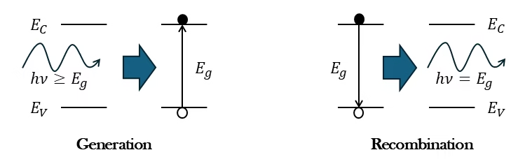
There are different mechanisms by which electron-hole pairs recombine and are generated. I will briefly describe the three possible processes without going much into detail. The first one is the recombination or generation via a “stepping-stone” in the bandgap, called Shockley-Read-Hall recombination-generation. The other two are band-to-band transitions, which means that the electron and the hole interact directly from band to band, without passing through an intermediate state. The energy that is released (absorbed) upon band-to-band recombination (generation) of an electron-hole pair can be transferred to (originate from) a photon or another free electron or hole. In the first case, the transition is called radiative, and in the latter case it is referred to as the Auger process.
In general, such recombinations leads to the generation of photons. This effect is used in devices like LEDs and laser diodes.
3.3 Direct and Indirect Band-gap semiconductors
In reality, the conduction band and valence band are not flat because their energy depends on the crystal momentum k. The band structure arises from the interaction of electrons with the periodic potential of the crystal lattice, leading to energy bands that vary with k. The reason they are often drawn as parabolas (near band extrema) is due to the effective mass approximation (which is quadratic):
\[E(k)\approx E_0 +\frac{\hbar^2k^2}{2m^*}\]
where m* is the effective mass of charge carriers. That is why you read about heavy and light holes in the conduction band, as they talk about different effective masses, but this I will not explain here.
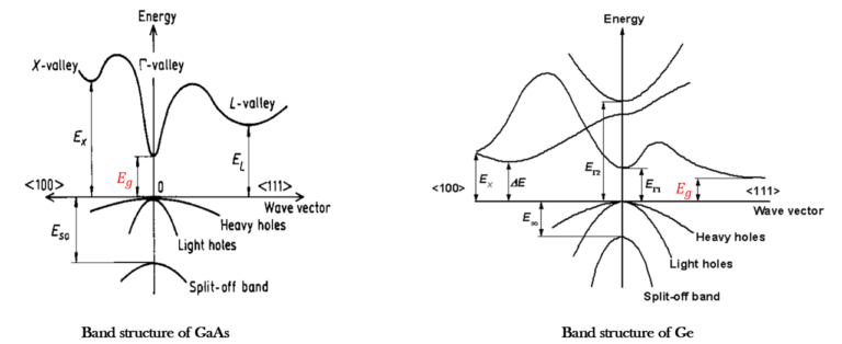
In a direct band-gap semiconductor, like GaAs, the minimum of the conduction band lies at the same k wave vector (k=0) than the maximum of the valence band. Since k is related to the momentum p of carriers according to the expression:
\[p=\hbar k,\]
the recombination of an electron from the conduction band with a hole in the valence band occurs without changing the momentum. This kind of radiative recombination is called a direct transition. During this transition, the energy lost by an electron is equal to Eg. The energy of the ohoton generated during this process is thus given by:
\[h\nu=E_g.\]
For an indirect band-gap material, the minimum of the conduction band and the maximum of the valence band lie at different k-values. When an electron and hole recombine in an indirect band-gap semiconductor, ohonos must be involved to conserve momentum. Atoms vibrate about their mean position at a finite temperature. These vibrations produce vibrational waves inside the crystal. Phonos are the quanta of these vibrational waves and they travel with a velocity of sound. Their wavelength is determined by the crystal lattice constant.
Why Direct Band-Gap for LEDs and Lasers?
The reason why direct vs indirect band-gap semiconductors is important is because in order to have efficient LED’s and LASER’s, one should choose materials having direct band gaps, such as compound semiconductor of GaAs, AlGaAs and so on. As this does not require additional momentum transfer (phonons are not required!).
The relationship between the wavelength and band gap is given by:
\[\lambda(\mu\text{m})=\frac{1.24(\text{eV}\mu\text{m})}{E_g(\text{eV})}\]
GaAs generates photons with a wavelength of 0.88 μm, corresponding to infrared range (at the limit of visible range). In order to produce photons in the visible range, GaAs can be doped with elements like P and In, producing complex alloys.
Florius
Hi, welcome to my website. I am writing about my previous studies, work & research related topics and other interests. I hope you enjoy reading it and that you learned something new.
More Posts