 Daily tech news
- First ever atomic movie reveals hidden driver of radiation damageResearchers have visualized atoms in motion just before a radiation-driven decay process occurs, revealing a surprisingly dynamic scene. Instead of remaining fixed, the atoms roam and rearrange, directly influencing how and when the decay unfolds. This “atomic movie” shows that structure and motion play a central role in radiation damage mechanisms. The findings could improve […]
- MIT scientists finally see hidden quantum “jiggling” inside superconductorsMIT physicists have built a powerful new microscope that uses terahertz light to uncover hidden quantum motions inside superconductors. By compressing this normally unwieldy light into a tiny region, they were able to observe electrons moving together in a frictionless, wave-like state for the first time. This discovery opens a new window into how superconductors […]
- A lab mistake at Cambridge reveals a powerful new way to modify drug moleculesCambridge scientists have discovered a light-powered chemical reaction that lets researchers modify complex drug molecules at the final stages of development. Unlike traditional methods that rely on toxic chemicals and harsh conditions, the new approach uses an LED lamp to create essential carbon–carbon bonds under mild conditions. This could make drug discovery faster and more […]
- Scientists just found a way to 3D print one of the hardest metals on EarthScientists have found a promising new way to manufacture one of industry’s toughest materials—tungsten carbide–cobalt—using advanced 3D printing. Normally, producing this ultra-hard material requires high-pressure processes that waste large amounts of expensive tungsten and cobalt. The new approach uses a hot-wire laser technique that softens the metals rather than fully melting them, allowing manufacturers to […]
- Scientists turn scrap car aluminum into high-performance metal for new vehiclesScientists at Oak Ridge National Laboratory have created a new aluminum alloy called RidgeAlloy that can turn contaminated car-body scrap into strong structural vehicle parts. Normally, impurities introduced during recycling make this scrap unsuitable for high-performance applications. RidgeAlloy overcomes that challenge, enabling recycled aluminum to meet the strength and durability standards required for modern vehicles. […]
- Electrons catapult across solar materials in just 18 femtosecondsElectrons in solar materials can be launched across molecules almost as fast as nature allows, thanks to tiny atomic vibrations acting like a “molecular catapult.” In experiments lasting just 18 femtoseconds, researchers at the University of Cambridge observed electrons blasting across a boundary in a single burst, far faster than long-standing theories predicted. Instead of […]
Category
Scaling beyond 100nm – Nanoelectronics Era
As silicon and silicon dioxide reach their scaling limits, engineers turn to high-k materials, metal gates, and new device architectures like FinFETs and SOI. These...
Scaling of CMOS: Microelectronics era
As CMOS technology shrank below 1 μm in the microelectronics era, high electric fields caused reliability issues like hot carrier effects. Techniques such as LATID...
Scaling of CMOS and its Issues
Dennard scaling revolutionized microelectronics by showing that reducing transistor size and voltage proportionally keeps power density constant. However, real-world limitations like subthreshold slope and interconnect...
CMOS Process Steps: 3um to 1.25um
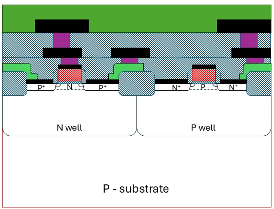
CMOS chips are made using a twin-well process, with precise tailoring of each well starting from a lightly doped substrate. Key production steps include using...
Basic nMOS Technology: Process Steps
NMOS fabrication involves key process steps like substrate selection, isolation, gate formation, and metallization. LOCOS isolation prevents unwanted current flow, while polysilicon gates enhance process...
The Physics and Technology of Extrinsic Semiconductors
Doping modifies a semiconductor by introducing donor or acceptor atoms, increasing free electron or hole concentration. This creates an n-type or p-type material, shifting the...


