 Daily tech news
- First ever atomic movie reveals hidden driver of radiation damageResearchers have visualized atoms in motion just before a radiation-driven decay process occurs, revealing a surprisingly dynamic scene. Instead of remaining fixed, the atoms roam and rearrange, directly influencing how and when the decay unfolds. This “atomic movie” shows that structure and motion play a central role in radiation damage mechanisms. The findings could improve […]
- MIT scientists finally see hidden quantum “jiggling” inside superconductorsMIT physicists have built a powerful new microscope that uses terahertz light to uncover hidden quantum motions inside superconductors. By compressing this normally unwieldy light into a tiny region, they were able to observe electrons moving together in a frictionless, wave-like state for the first time. This discovery opens a new window into how superconductors […]
- A lab mistake at Cambridge reveals a powerful new way to modify drug moleculesCambridge scientists have discovered a light-powered chemical reaction that lets researchers modify complex drug molecules at the final stages of development. Unlike traditional methods that rely on toxic chemicals and harsh conditions, the new approach uses an LED lamp to create essential carbon–carbon bonds under mild conditions. This could make drug discovery faster and more […]
- Scientists just found a way to 3D print one of the hardest metals on EarthScientists have found a promising new way to manufacture one of industry’s toughest materials—tungsten carbide–cobalt—using advanced 3D printing. Normally, producing this ultra-hard material requires high-pressure processes that waste large amounts of expensive tungsten and cobalt. The new approach uses a hot-wire laser technique that softens the metals rather than fully melting them, allowing manufacturers to […]
- Scientists turn scrap car aluminum into high-performance metal for new vehiclesScientists at Oak Ridge National Laboratory have created a new aluminum alloy called RidgeAlloy that can turn contaminated car-body scrap into strong structural vehicle parts. Normally, impurities introduced during recycling make this scrap unsuitable for high-performance applications. RidgeAlloy overcomes that challenge, enabling recycled aluminum to meet the strength and durability standards required for modern vehicles. […]
- Electrons catapult across solar materials in just 18 femtosecondsElectrons in solar materials can be launched across molecules almost as fast as nature allows, thanks to tiny atomic vibrations acting like a “molecular catapult.” In experiments lasting just 18 femtoseconds, researchers at the University of Cambridge observed electrons blasting across a boundary in a single burst, far faster than long-standing theories predicted. Instead of […]
Category
Mapping the Cosmic Microwave Background
The Mollweide projection preserves area while unfolding a spherical sky into two dimensions, allowing full-sky CMB data to be visualized and analyzed consistently....
IGBT vs MOSFET: How to Choose the Right Power Switch
This article compares IGBTs and MOSFETs for power electronics applications It covers efficiency trade-offs, conduction and switching losses, voltage/current guidelines, structural differences (such as body...
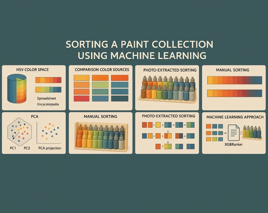
Sorting Vallejo Paints with Machine Learning
This article explores how to visually sort color collections using both statistics and machine learning. After experimenting with PCA for dimensionality reduction and simple color...
K-Means Clustering for Colors
Discover how K-Means clustering helps analyze and evaluate Vallejo Model Color paints using Rembrandt’s masterpiece as a case study. Learn to identify gaps in your...
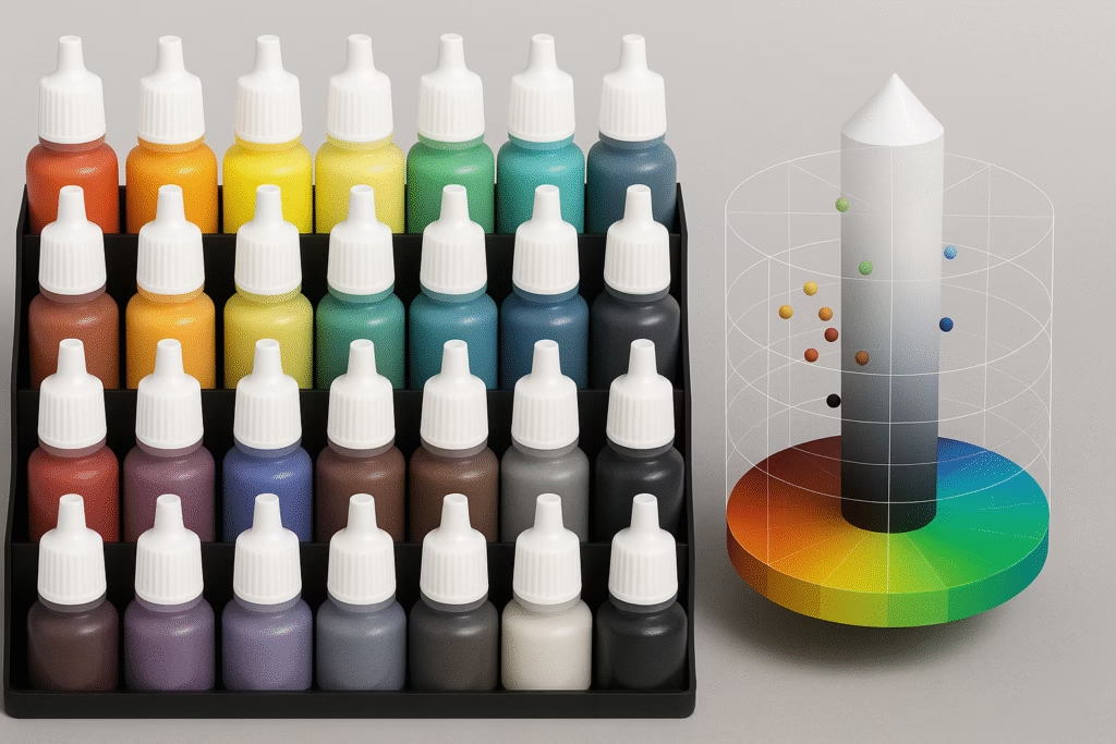
HSV color chart for vallejo paint
Curious how your paints stack up in color space? I analyzed my Vallejo paints by converting RGB values to HSV, visualizing them in 3D, and...
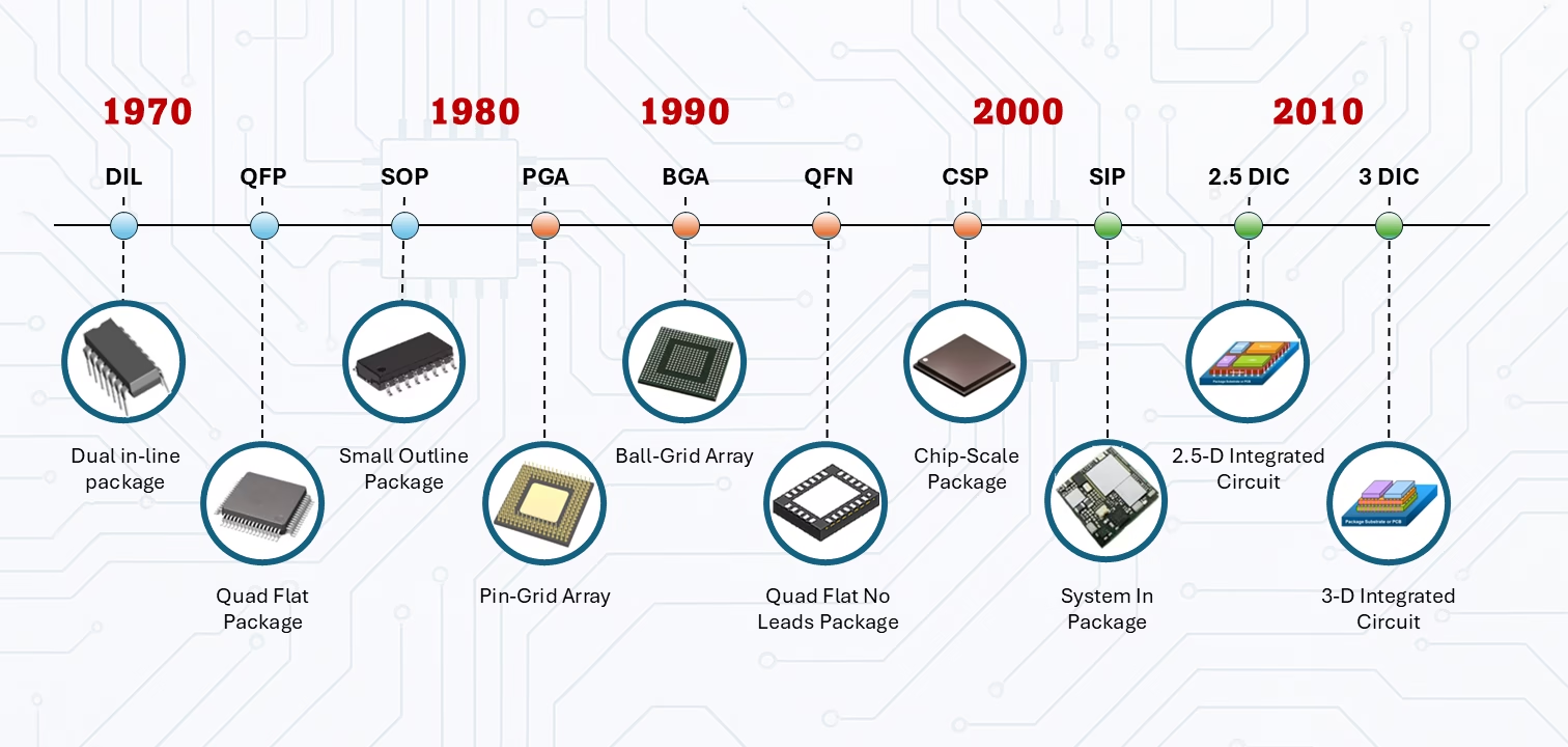
Semiconductor Packaging Technology
Wire bonding and flip-chip packaging represent two fundamental approaches to chip interconnection. While wire bonding offers simplicity and cost benefits, flip-chip allows higher density and...


