The Insulated Gate Bipolar Transistor, also called IGBT, is something of a cross between a metal-oxide-semiconductor field-effect transistor (MOSFET) with a bipolar junction transistor (BJT). It can be used as a semiconductor switching device. The IGBT takes the insulated gate technology of a MOSFET (hence the first part of the name) and combines it with the output performance characteristics of a BJT, (hence the second part of the name). As a result, the IGBT has the output switching characteristics of the BJT, but can be voltage controlled, such as a MOSFET. It takes the best of both worlds.
It can be used in small amplifying circutis, replacing BJTs and MOSFETs. But because it has a very low “on-state” resistance, lower then the other two, it has very low power loss ( ). Due to this, and the fact that it is capable of handing large currents (1000+ Amps) with basically zero gate current, it is mainly used in power electronics, such as power supplies and inverters. Even though high power BJTs exist, their switching speed is much lower than these IGBTs, making this the ideal device to use.

The main difference between the construction of an IGBT and a MOSFET, is the additional  substrate layer, known as the injection layer. This layer is heavily doped with an intensity of
  per cm
 . The thickness of the
  is proportional to its voltage blocking capacity. The
  layer on top of that, is known as the body of the IGBT.
In the left figure, you find the typical Non-Punch Through (NPT) IGBTs, which have a symmetrical breakdown voltage characteristics i.e. their forward and reverse breakdown voltage are equal. Due to this, they are used in high voltage AC circuits.
Another type is the Punch Through (PT) IGBTs, that have an additional  buffer layer that is included in the stack, which creates an asymmetric voltage blocking capability i.e. their forward and reverse breakdown voltages are different. These PT IGBTs are unidirectional, and are therefore used in DC circuits such as inverters and high voltage chopper circuits.
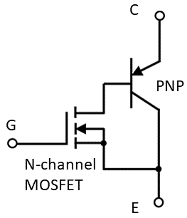
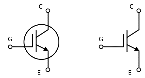
The equivalent circuit shows an N-channel MOSFET that drives a PNP bipolar transistor in a darlington configuration. Intuitively, you can see that the voltage across the IGBT is one diode voltage higher than when using a single N-channel MOSFET on its own. You can measure that the on-state voltage across the IGBT is at least one diode drop (~0,7 V). However, when equally comparing an IGBT vs a MOSFET of the same size, at same temperature and same current, the IGBT will have a lower on-state voltage. The reason for that is, that in IGBTs the current flow consists of both holes and electrons, compared to MOSFET, which is a majority carrier device only. Thus, the injection of minority carriers in IGBTs result in a reduction of on-state voltage and it is one of the major advantages of IGBTs over power MOSFETs.
The downside of using IGBTs is the slower switching speed. When turning off the device, the flow of electrons can be stopped rather quickly by reducing the gate-emitter voltage. But the holes, are still left in the drift region and takes longer to recombine. The rate of recombination can be controlled by adding an additional buffer layer. This buffer layer will quickly absorb holes during the turn off phase. IGBTs with this additional buffer layer are called Punch-Through IGBTs, as discussed in the previous section.
The second disadvantage is the possibility of latchup, where the IGBT can no longer be shut down by the gate voltage. It happens when you are using the device outside of its specs. As example, when too much current runs thruogh the device, it can destroy it due to overheating, because it can not be turned off. Similarly, when switching large voltages in short periods, the IGBT can also derail. Normally, by staying within safe operating ranges, you will not trigger latchups
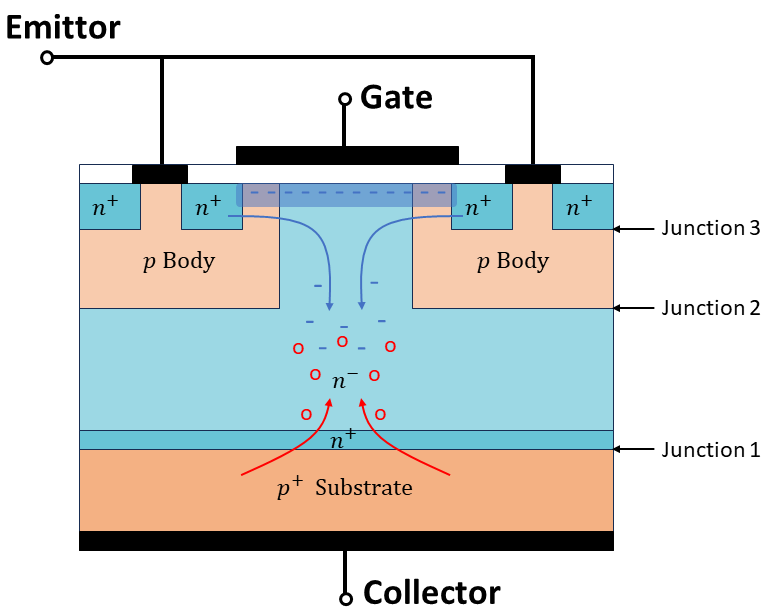
In the forward blocking mode, there is no current flowing between the collector and emittor, it is also called the off-state. To get the IGBT in the forward blocking mode, we need to set a positive voltage on the collector with respect to the emitter and put zero voltage on the Gate terminal. This will effect the 3 junctions that exist in the IGBT. Junction 1 and 3 will get into forward bia. However, junction 2 is in reverse bias, preventing the flow of current.
When we increase the gate voltage  , so it is more positive than the emitter voltage, an inversion layer (a capacitive effect) is created near the metal gate layer. This layer creates a channel, that shorts the and regions. The doped part has an excess of electrons that get pushed into the region, also called the drift region. The amount of electrons will lower the potention for the holes (shown as red circles) to flow from the substrate into this region as well, as they get attracted by the negative electrons. This ultimately leads to a plasma of holes, which attracts more electrons, etc. At this point everything is forward biased and it is in conducting mode.
If, at this moment, you’d remove the voltage from the gate. The capacitance on the gate will keep the inversion layer and the IGBT continues to conduct. Only if you let the gate capacitance discharge, by grounding it, will the IGBT stop conducting.
 ) of 1.8V at 15A. Interestingly, at 25 degrees Celsius, it can handle a current of 30A.
 ) indicates whether a heatsink is necessary.
 ), to turn on the device. It is not uncommon to have a gate voltage
  . Normally, the higher the gate voltage, the higher the current through the device.
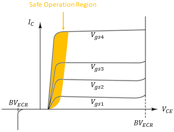
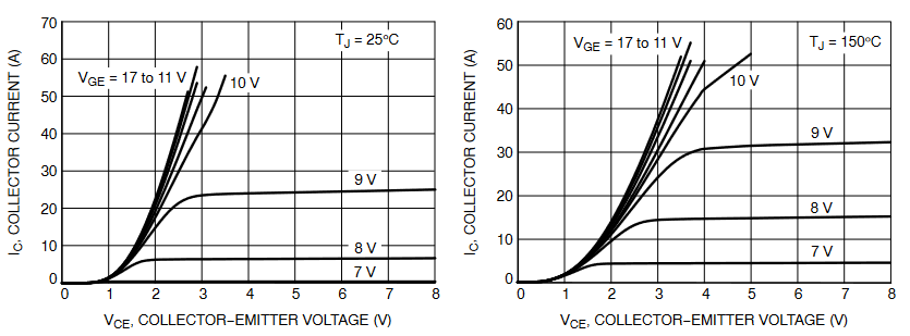
Figure 5 depicts a typical IGBT characteristic curve, highlighting the safe operating region (in yellow) just before over-saturation begins. Beyond this point, the IGBT enters a runaway behavior, where the current remains constant despite an increase in  , which can be detrimental to the circuit as more heat is being dissipated. This graph provides valuable insight into the safe operating current for a given gate voltage. However, many datasheets may not include such an extended version and instead only present the safe operating region for various temperatures, as can be seen in Figure 6.