
 Daily tech news
- A strange quantum effect could power future electronicsRice University physicists confirmed that flat electronic bands in kagome superconductors aren’t just theoretical, they actively shape superconductivity and magnetism. This breakthrough could guide the design of next-generation quantum materials and technologies.
- Room-temperature quantum breakthrough freezes motion without coolingETH Zurich scientists have levitated a tower of three nano glass spheres using optical tweezers, suppressing almost all classical motion to observe quantum zero-point fluctuations with unprecedented precision. Achieving 92% quantum purity at room temperature, a feat usually requiring near absolute zero, they have opened the door to advanced quantum sensors without costly cooling.
- Tiny gold “super atoms” could spark a quantum revolutionScientists have found that microscopic gold clusters can act like the world’s most accurate quantum systems, while being far easier to scale up. With tunable spin properties and mass production potential, they could transform quantum computing and sensing.
- Scientists unveil bioplastic that degrades at room temperature, and outperforms petroplasticsPlastic pollution is a mounting global issue, but scientists at Washington University in St. Louis have taken a bold step forward by creating a new bioplastic inspired by the structure of leaves. Their innovation, LEAFF, enhances strength, functionality, and biodegradability by utilizing cellulose nanofibers, outperforming even traditional plastics. It degrades at room temperature, can be […]
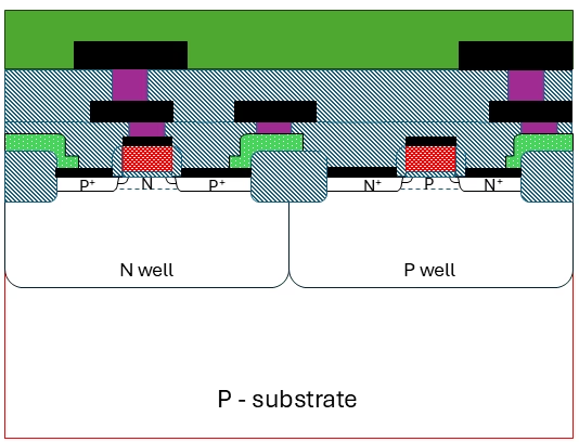
- Building electronics that don’t die: Columbia's breakthrough at CERNDeep beneath the Swiss-French border, the Large Hadron Collider unleashes staggering amounts of energy and radiation—enough to fry most electronics. Enter a team of Columbia engineers, who built ultra-rugged, radiation-resistant chips that now play a pivotal role in capturing data from subatomic particle collisions. These custom-designed ADCs not only survive the hostile environment inside CERN […]
- Digital twins are reinventing clean energy — but there’s a catchResearchers are exploring AI-powered digital twins as a game-changing tool to accelerate the clean energy transition. These digital models simulate and optimize real-world energy systems like wind, solar, geothermal, hydro, and biomass. But while they hold immense promise for improving efficiency and sustainability, the technology is still riddled with challenges—from environmental variability and degraded equipment […]